Clear Sky Science · en
A novel observation of negative differential resistance in a standard CMOS transistor and its application to a compact frequency doubler
Turning a Tiny Switch into a Signal Shaper
Modern electronics are built from unimaginably small switches called transistors. This study shows that a completely standard kind of transistor, already used in mass-produced computer chips, can do more than simply turn current on and off. Under the right conditions, it can reshape electrical signals in a useful way, opening the door to smaller, more energy-efficient circuits for communications and sensing.
A Curious Dip in the Current
Most of the time, when you push harder on an electrical device by raising the voltage, more current flows. In this work, the researchers focus on an unusual exception called negative differential resistance, where the current briefly drops even as the voltage rises. This quirk has been seen before in exotic components and special materials, but rarely in the workhorse transistors used in everyday chips. Finding this behavior in a mainstream technology means designers could gain new functions without changing the manufacturing process.
How a Common Transistor Is Built
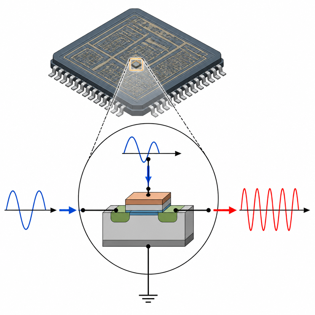
The team studies a fully depleted silicon-on-insulator transistor, a refined version of the basic switch used in many modern processors. In this design, an ultrathin silicon layer sits on top of an insulating layer, with a metal gate above that controls how easily electrons move between the source and drain. This structure is prized for its low leakage, strong control over current, and suitability for shrinking to very small sizes. These same traits also make it a clean platform for spotting subtle nonlinear behaviors such as the unexpected drop in current the team set out to explore.
Two Different Ways the Current Can Fall
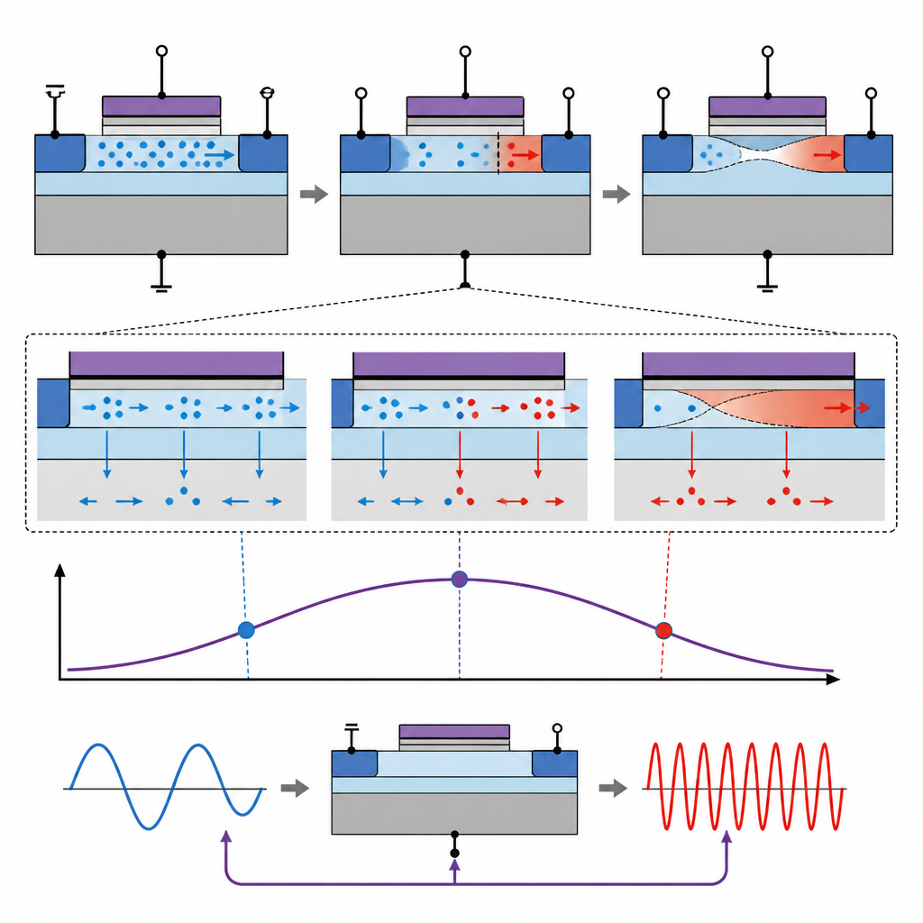
By carefully measuring how current responds to changing voltages at different terminals of the device, the researchers uncovered two distinct kinds of negative differential resistance. At the drain terminal, which collects electrons leaving the channel, the effect appears only at very high voltages. Here, some electrons gain enough energy to become “hot” and get trapped in material near the drain. These trapped charges distort the local electric field and temporarily reduce the current. Noise measurements, computer simulations, and temperature tests all support this picture: as heat makes it harder for electrons to become hot, the dip in current fades away.
A Stable Sweet Spot in the Body Terminal
The second and more useful effect shows up in the body terminal, the hidden region of silicon beneath the channel. When the drain voltage is high and the gate voltage is swept, the body current first rises sharply and then falls, forming a well-defined peak. At low gate voltage, a leakage effect near the drain dominates. As the gate voltage increases into a middle range, the sideways electric field becomes strong enough that electrons trigger impact ionization, creating extra charge and boosting the body current. Pushing the gate voltage higher still lowers the resistance of the channel, softening that sideways field and cutting back the extra charge creation, so the current drops. This clean rise-and-fall pattern is highly repeatable across many devices and over many test cycles, with a remarkably large ratio between the peak and valley currents.
From Strange Behavior to Useful Function
Because the body current responds to the gate voltage in a sharp, predictable way, the team used this nonlinearity to build a simple frequency doubler using just one transistor and an external resistor. Feeding in a low-frequency sine wave at the gate produces an output signal whose main component is at twice the original frequency, and this doubling effect can be switched on or off by adjusting the drain voltage. While the demonstration operates at modest frequencies suited to sensing applications, it shows that standard chip technology can host compact, reconfigurable signal-processing blocks without exotic materials or complex multi-device circuits. In everyday terms, the work turns a basic switch into a tiny on-chip tool for reshaping signals, while also deepening our understanding of how current flows in advanced transistor structures.
Citation: Kwak, B., Cho, Y., Han, C. et al. A novel observation of negative differential resistance in a standard CMOS transistor and its application to a compact frequency doubler. Microsyst Nanoeng 12, 186 (2026). https://doi.org/10.1038/s41378-026-01276-3
Keywords: negative differential resistance, CMOS transistor, FDSOI, frequency doubler, nonlinear electronics