Clear Sky Science · en
Facile, etch-free atomic layer-coated resist templates for rapid prototyping of efficient visible metasurfaces
Flat Lenses for Everyday Light
Modern gadgets—from smartphones to virtual reality headsets—are packed with cameras and displays that all rely on tiny lenses and mirrors to steer light. Shrinking these optical parts without sacrificing performance is a huge challenge. This paper introduces a simpler, faster way to make “metasurfaces,” ultra-thin layers covered with tiny structures that can bend and shape visible light with high efficiency. The work points toward cheaper, more compact optics for future screens, sensors, and imaging systems.
From Thick Optics to Ultra-Thin Patterns
Traditional high-performance flat optics in the visible range are built from thick layers of special transparent materials. Engineers first deposit a heavy film of a high-index material like titanium dioxide, then pattern it with a resist, add a hard mask, and finally carve out the desired shapes by high-energy plasma etching. Each of these steps demands expensive tools, vacuum systems, and careful alignment. While this approach can deliver impressive performance, it is slow, costly, and not well suited for rapid testing of new designs or for use on unconventional substrates such as flexible plastics.
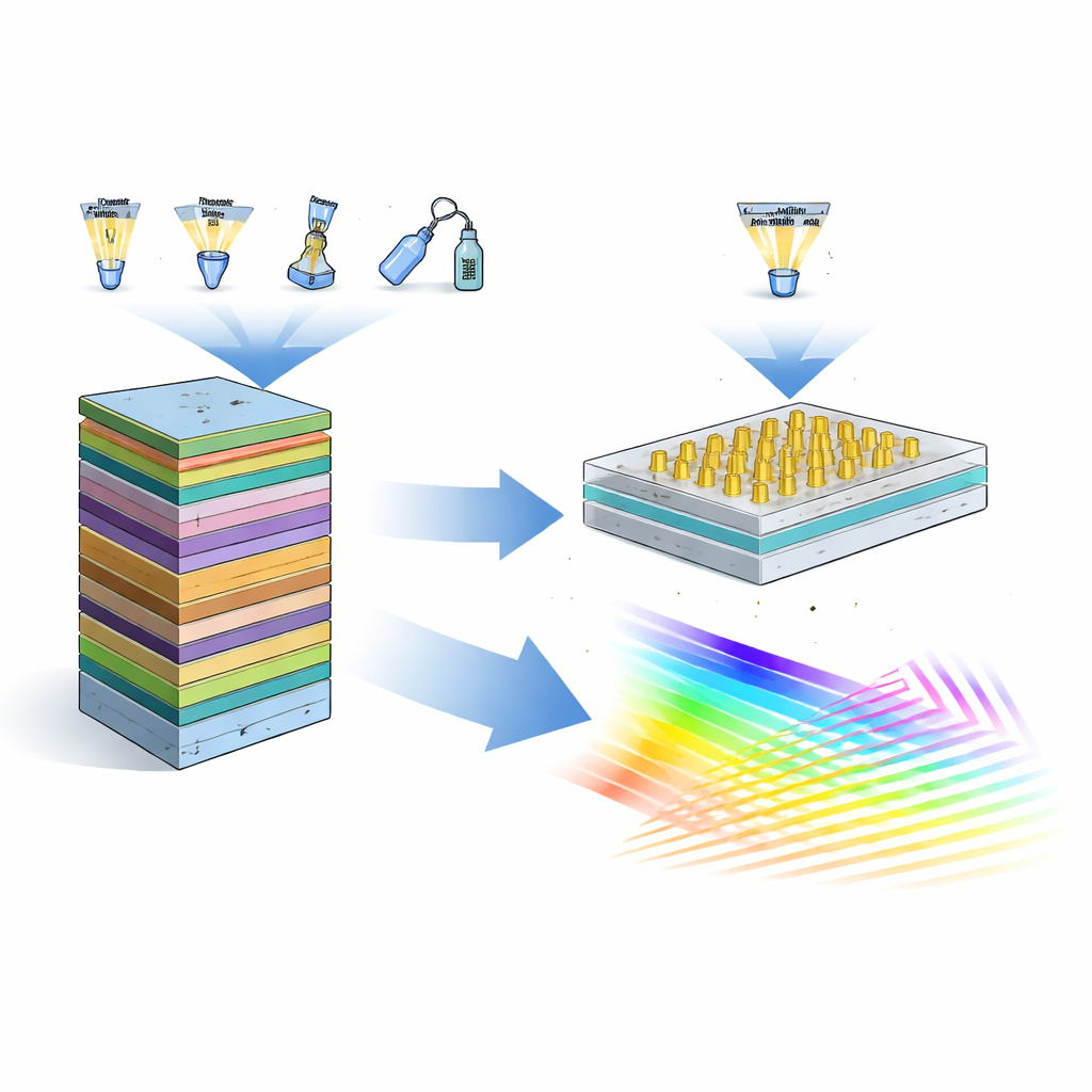
Using the Drawing Ink as the Device Itself
The authors simplify this entire process by turning the patterning resist—the “ink” normally used only to draw shapes—into the working optical material itself. They spin-coat a common electron-beam resist onto a glass wafer and directly write the nanoscale pillars that form the metasurface in a single exposure step. After development, these slender polymer pillars stand on the surface without any etching or lift-off. Achieving this requires careful tuning of how the resist is exposed and developed, along with a clever drying method that blows gas from behind the wafer and uses a graded rinse. This reduces the capillary forces that would otherwise topple the tiny pillars like wet blades of grass.
Boosting Light Control with a Thin Shell
On its own, the resist is too weak a guide for visible light because its refractive index is modest. To fix this, the team envelops each polymer pillar in an ultrathin shell of titanium dioxide applied by atomic layer deposition, a technique that coats complex shapes evenly, atom by atom. Just 28 nanometers of this high-index material is enough to dramatically increase how strongly light is confined and redirected. Through computer simulations, they identify pillar sizes and shell thicknesses that push the cross-polarized transmission—the useful output channel for their design—to over 90 percent near green light, while also working across the broader visible spectrum.
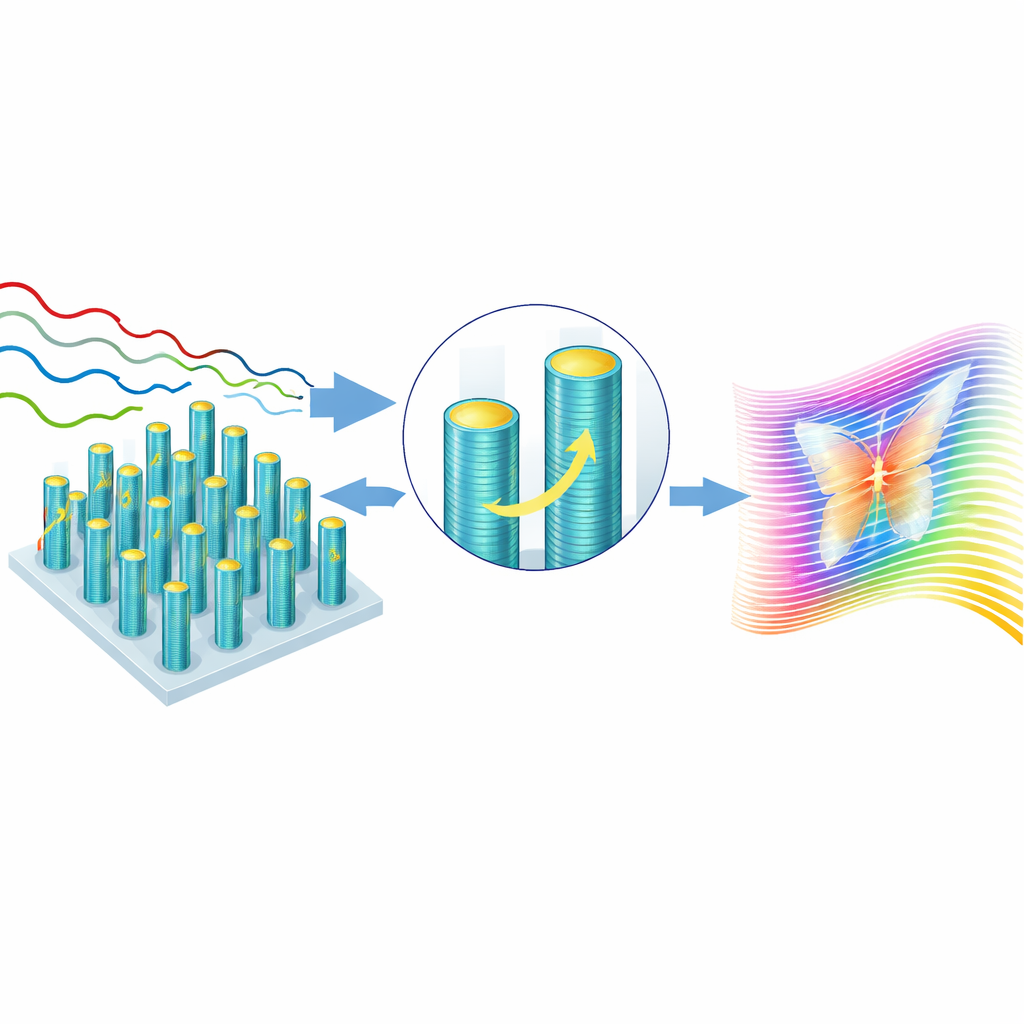
Writing Holograms with Rotated Pillars
To showcase what these hybrid pillars can do, the researchers design holograms using a concept called geometric phase. Instead of changing the size of each pillar, they rotate identical pillars across the surface. When circularly polarized light hits these rotated elements, the rotation angle directly maps to the phase shift imposed on the outgoing light. Using an iterative algorithm, they convert a desired image into a phase map and then into a pattern of pillar orientations. Experiments at blue, green, and red laser wavelengths show that uncoated resist structures produce dim, low-contrast holograms. After adding the titanium dioxide shell, the holograms become far brighter and cleaner, with measured efficiencies increasing by about a factor of four and reaching more than 70 percent at green wavelengths.
Simple Steps Toward Future Flat Optics
In everyday terms, this work turns a complicated, multi-step carving process into something closer to drawing and spray-coating, while still delivering top-tier optical performance. By using the resist both as the pattern and the material, then boosting it with a thin high-index shell, the authors create efficient, broadband metasurfaces without harsh etching steps. Their method is compatible with different resists and substrates and can be adapted to other colors of light by scaling the structures and choosing suitable coatings. This streamlined approach could help move flat optical elements from laboratory curiosities toward widespread use in next-generation displays, wearable devices, and compact imaging systems.
Citation: Seong, J., Jeon, Y., Lee, S. et al. Facile, etch-free atomic layer-coated resist templates for rapid prototyping of efficient visible metasurfaces. Microsyst Nanoeng 12, 127 (2026). https://doi.org/10.1038/s41378-026-01238-9
Keywords: metasurfaces, flat optics, holography, nanofabrication, titanium dioxide coating