Clear Sky Science · en
Large-area metal-integrated grating electrode achieving near 100% infrared transmission
Sharper Eyes for Invisible Light
Many of today’s most advanced technologies—from thermal cameras and night-vision goggles to self‑driving car LiDAR and infrared lasers—depend on parts that must both carry electrical current and let infrared light pass through. Unfortunately, materials that conduct electricity well usually block or reflect a lot of this light. This paper presents a new way to build an infrared “window” that behaves almost like a perfect pane of glass for mid‑ to far‑infrared light while still acting as a powerful metal electrode.
The Challenge of Seeing in the Infrared
Transparent conductive electrodes are the clear, metal-like layers that sit on the surface of LEDs, lasers, and sensors. They have to do two opposite things at once: move large electrical currents and stay transparent. In the visible range—what our eyes can see—scientists have developed good solutions, such as indium tin oxide coatings for phone screens and solar cells. But in the mid‑ and far‑infrared, where thermal cameras and many advanced detectors operate, these same materials start to behave badly. Their electrons absorb and reflect infrared light, so simply adding a conductive film on top of a semiconductor wafer can cut transmission well below what a bare surface would allow.
A New Kind of Metal–Glass Fence
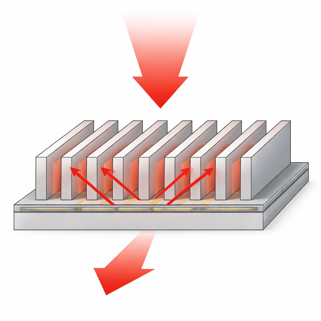
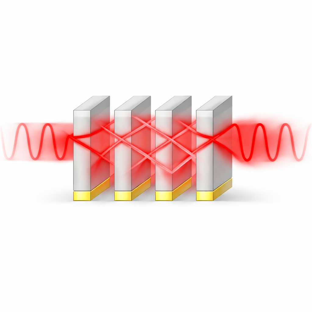
The authors tackle this problem by reshaping, rather than replacing, the metal. Instead of laying down a flat sheet, they carve the surface of a gallium arsenide (GaAs) wafer into a dense picket‑fence of ridges and then embed narrow gold stripes at the bottoms of the grooves. This pattern—called a metal‑integrated monolithic high‑contrast grating—acts like a finely engineered fence for light. For mid‑ to far‑infrared wavelengths, the structure behaves not as separate wires and gaps, but as a single, carefully tuned optical layer with an “effective” refractive index lower than the bulk semiconductor. In this regime, the patterned surface mimics a high‑quality anti‑reflection coating while the buried gold still provides an easy path for electrical current.
Guiding Light with Hidden Resonances
Through detailed simulations, the team shows that the grating can be tuned so that both major polarizations of light experience a gentle, cavity‑like resonance known as a Fabry–Perot mode. Because the electric field is mostly concentrated in the semiconductor ridges for one polarization and in the air gaps for the other, very little of it penetrates into the gold. That means absorption in the metal stays remarkably low, even though there is a lot of gold present. By adjusting the ridge height and the ratio of ridge width to period, the researchers identify conditions where these resonances line up for both polarizations in a higher‑order “transmission band,” allowing almost all unpolarized infrared light to pass through.
Turning Theory into a Working Device
The team then fabricates this grating over more than a square centimeter of GaAs using industrially compatible techniques: electron‑beam lithography and plasma etching to form deep, narrow grooves, followed by a carefully controlled gold deposition. Microscopy confirms that the real structure matches the design closely. Measurements with a vacuum infrared spectrometer show that at a wavelength of about 7 micrometers, the device transmits 94% of unpolarized light—about 35% more than the theoretical limit for a simple flat GaAs–air surface. At the same time, clever electrical test structures reveal an extraordinarily low sheet resistance of just 2.8 ohms per square, rivaling or beating the best infrared electrodes reported to date. Infrared imaging experiments further show that a scene viewed through the new electrode appears noticeably brighter than through bare GaAs, underscoring the improved transmission in practice.
Why This Matters for Future Infrared Tech
By combining near‑perfect transparency with extremely high electrical conductivity, this metal‑integrated grating breaks the usual trade‑off that has long limited transparent electrodes, especially in the infrared. The design can be adjusted to different wavelengths, integrated directly on top of semiconductor devices, and fabricated using scalable lithography methods already used in chipmaking. This makes it a strong candidate for next‑generation infrared lasers, LEDs, and detectors that need both high optical throughput and high current density, as well as for transparent heaters and electromagnetic shields that must stay clear to thermal imaging. In simple terms, the work offers a new kind of “invisible metal” for infrared devices—one that lets almost all the desired light through while still doing the heavy lifting of carrying electrical power.
Citation: Bogdanowicz, K., Głowadzka, W., Smołka, T. et al. Large-area metal-integrated grating electrode achieving near 100% infrared transmission. Light Sci Appl 15, 195 (2026). https://doi.org/10.1038/s41377-026-02270-0
Keywords: infrared transparent electrode, high contrast grating, gallium arsenide, plasmon-free metal optics, optoelectronic devices