Clear Sky Science · en
Plasmonic metamaterials for multi-effect enhancement: bridging optical, electronic, thermal, and acoustic domains
Light That Does More Than Shine
Imagine tiny metal structures so small that they can grab light, squeeze it, and turn it into other useful forms of energy right where it is needed. This review article explores such structures—plasmonic metamaterials—and shows how they can boost not just light-based signals, but also electrical currents, heat, and sound waves. For readers interested in future medical tests, cleaner energy, faster computers, or new kinds of data storage, these miniature platforms offer a glimpse of how one smart surface could power many technologies at once.
Building Tiny Light Antennas
At the heart of plasmonic metamaterials are “nano-antennas”: metal or conductive structures smaller than the wavelength of light. When light hits metals like gold, silver, or aluminum at the right color, the metal’s electrons slosh back and forth in unison, creating a surface wave called a plasmon. By shaping the metal into spheres, rods, flat patterns, or three‑dimensional lattices, scientists can tune how strongly and where these waves form. The article explains how different material families—metals, semiconductor particles, atomically thin sheets like graphene, and even conductive polymers—can all host plasmons. It also contrasts bottom‑up growth methods, such as chemical self‑assembly and DNA‑guided construction, with top‑down approaches borrowed from the chip industry, like electron‑beam writing and nanoimprint stamping. Together, these techniques let engineers “draw” intricate plasmonic patterns with nanometer precision.
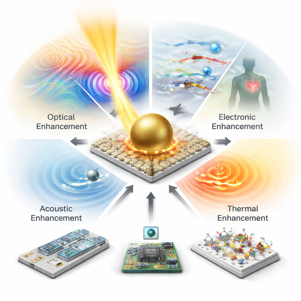
Four Ways to Supercharge Energy at the Nanoscale
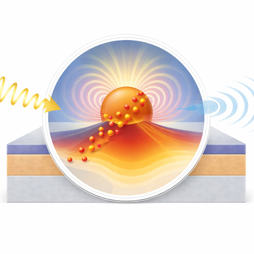
When these nano‑antennas resonate, they concentrate light into extremely small volumes, which triggers four major effects. First, optical enhancement: local fields near the metal can be thousands of times stronger than the incoming beam, boosting weak signals such as Raman scattering, infrared absorption, and fluorescence from molecules. Second, electronic enhancement: excited plasmons can decay into “hot” electrons energetic enough to jump into a nearby semiconductor, creating new paths for solar energy conversion and ultrafast photodetectors. Third, thermal enhancement: non‑radiative decay heats the metal and its surroundings, enabling ultra‑precise light‑to‑heat conversion for printing, therapy, and micro‑fluidic control. Fourth, acoustic enhancement: in structures such as graphene suspended over a metal, special “acoustic plasmons” form and couple strongly to vibrations, improving infrared sensing and even revealing subtle quantum properties of metal surfaces.
From Sensors and Cameras to Catalysts and Circuits
Because all four effects can occur in the same place, a single plasmonic surface can act as a highly versatile “conversion cell”. The review surveys how this concept is being used across many fields. In chemical and biomedical sensing, nanostructured metals amplify molecular fingerprints in visible and infrared light, enabling label‑free detection of viruses, cancer markers, and battery by‑products. For imaging, plasmonic particles brighten fluorescent probes and strengthen photoacoustic echoes, helping locate tiny tumors deep in tissue while also serving as heaters for targeted therapy. In energy and chemistry, hot carriers from metal particles help split molecules like hydrogen at lower temperatures or steer reactions along more selective pathways. On chips, plasmonic elements shrink lasers, modulators, detectors, and logic functions to far below the usual size limit set by the wavelength of light, pointing toward ultracompact optical circuits that work alongside conventional electronics.
Hiding, Storing, and Computing with Color
Beyond sensing and medicine, the article highlights more futuristic uses where information itself is encoded in plasmonic responses. Carefully designed nano‑patterns can produce angle‑ and polarization‑dependent colors that act as invisible barcodes or encrypted images, only revealed under special viewing conditions. Other schemes use changes in luminescence or structural color as rewritable “bits” for dense optical data storage. Because these effects can be tuned by geometry, material choice, or applied signals, a single metasurface can multiplex several layers of hidden messages. The same design tools also support “in‑sensor computing”, where a plasmonic chip doesn’t just measure a signal but begins to analyze it optically—performing simple operations like filtering or pattern recognition before any electronics step in.
Where This Technology Is Headed
The authors conclude that plasmonic metamaterials are evolving into a general platform for managing light, charge, heat, and sound in one tightly integrated system. To move from lab demonstrations to everyday devices, researchers must still tackle metal losses, scalable manufacturing, and the challenge of combining several enhancement pathways in one stable design. Looking forward, the review points to emerging directions such as quantum‑level plasmonic devices, new low‑loss materials, and machine‑learning‑guided design. For the lay reader, the key message is that these tiny metal architectures could underpin a new generation of smart surfaces—ones that see, think, communicate, and even treat disease, all by sculpting how light behaves at the smallest scales.
Citation: Zhou, H., Li, D., Wang, Y. et al. Plasmonic metamaterials for multi-effect enhancement: bridging optical, electronic, thermal, and acoustic domains. npj Metamaterials 2, 14 (2026). https://doi.org/10.1038/s44455-026-00022-z
Keywords: plasmonic metamaterials, nanoscale sensing, hot electrons, photothermal therapy, integrated photonics