Clear Sky Science · en
Achromatic metalens for visible and infrared band: a unified four-paradigm framework
A New Kind of Flat Lens
Modern cameras, phones, telescopes, and AR/VR headsets all depend on carefully stacked glass lenses to form sharp, colorful images. These stacks are bulky and tricky to manufacture, and they still struggle with color blur, where reds, greens, and blues do not quite focus in the same place. This review explains how a new class of ultra-thin “metalenses,” built from tiny patterns on flat surfaces, could shrink complex optics into a single chip-sized element while keeping images clear across colors from visible light to the infrared.
Why Color Blur Is So Hard to Fix
In any lens, light of different colors bends by different amounts. Traditional curved glass lenses tend to focus blue light closer and red light farther away, so engineers combine multiple glass pieces to cancel this effect. Metalenses behave in the opposite way: because they are diffractive, longer wavelengths tend to focus closer than shorter ones. To make matters harder, both the material and the fine geometry of the nanostructures affect how each color travels. When you want a large lens that works across a wide band of colors with strong focusing power, these effects pile up and create strict trade-offs between how big, how sharp, how efficient, and how broadband the lens can be.
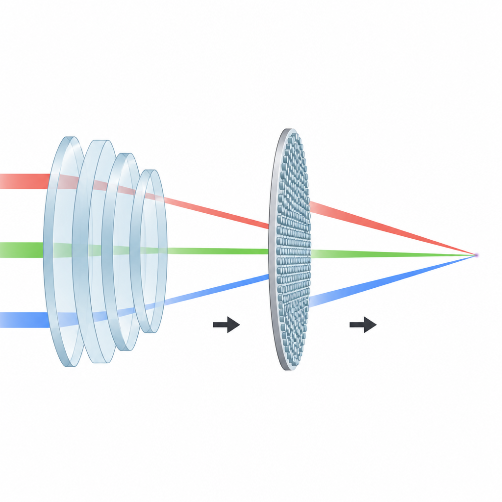
Four Main Strategies for Flat, Color-True Lenses
The authors group all current ideas for “achromatic” metalenses, which bring many colors to the same focus, into four main strategies. The first, dispersion engineering, carefully shapes the nanostructures so that their color delay counteracts natural dispersion, often by tuning both the phase and arrival time of light across the surface. The second, algorithm-aided design, uses heavy computation and machine learning both to search for better nanostructure patterns and, later, to clean up images digitally. The third, architecture modification, changes how the metalens sits in a larger system: using two flat layers instead of one, arrays of many small lenses, or a hybrid of a conventional lens plus a correcting metalens. The fourth, wavefront engineering, deliberately stretches the focus along the viewing direction so different colors share a long “in-focus” zone that software can then sharpen.
The Role of Computing and Smart Layouts
Because each nanostructure is tiny and sensitive, perfect designs on a computer often underperform once fabricated. The review shows how inverse design algorithms can build in manufacturing rules from the start, such as minimum feature sizes or allowable sidewall angles, to reduce this gap. At the same time, image-processing methods treat the metalens not as a perfect imaging element but as a predictable encoder that can be decoded later. Calibrated filters, neural networks, and lookup tables can remove color fringes, extend depth of field, and correct off-axis blur without adding more glass. Double-layer layouts, arrays of many small lenses, and hybrid metalens-plus-glass systems further relax the demands on any single patterned surface while still delivering wide fields of view and large apertures.
From Tiny Prototypes to Wafer-Scale Devices
A key question is not just whether achromatic metalenses can work in principle, but whether they can be manufactured at useful sizes and costs. The authors review studies that map the maximum lens radius to its color range and focusing strength, and then connect these physical limits to real fabrication tools. Electron-beam writing can draw extremely fine patterns but becomes slow and expensive for centimeter-scale apertures with billions of features. Instead, deep-ultraviolet stepper lithography and nanoimprint techniques can pattern entire wafers in parallel, while keeping alignment errors and layer thickness variations small enough for good optical performance. The review argues that combining moderate-aspect-ratio designs, double-layer or hybrid architectures, and computational correction offers the most realistic path to large, broadband, and efficient flat lenses.
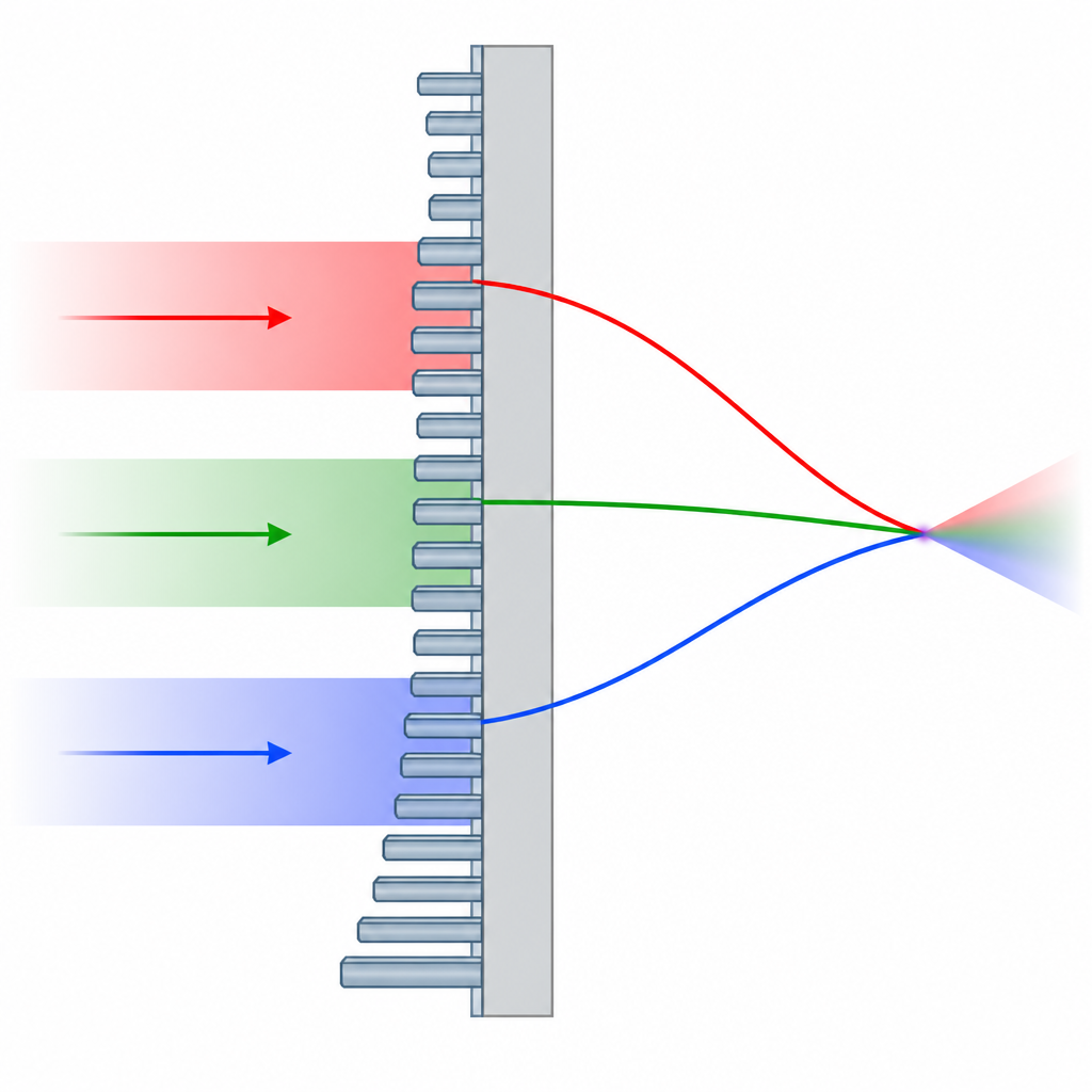
What This Means for Future Devices
Ultimately, the article concludes that there is no single trick that will make a perfect flat lens that works from visible to infrared over centimeter scales. Instead, practical achromatic metalenses will come from co-design: matching tailored nanostructures with smart algorithms, system layouts, and scalable manufacturing. By sharing a unified four-paradigm framework, the authors provide a roadmap for engineers to choose the right mix of approaches for applications like compact microscopes, thermal cameras, sensors, and AR/VR headsets. If these combined strategies succeed, tomorrow’s imaging systems could replace bulky lens stacks with thin, chip-like optics that keep colors in focus across a wide range of wavelengths.
Citation: Dong, G., Yan, J. Achromatic metalens for visible and infrared band: a unified four-paradigm framework. npj Nanophoton. 3, 28 (2026). https://doi.org/10.1038/s44310-026-00127-3
Keywords: achromatic metalens, flat optics, chromatic aberration, computational imaging, nanophotonics