Clear Sky Science · en
Stable and eco-friendly inorganic lead-free perovskite solar cells: structural, electronic, and defect engineering
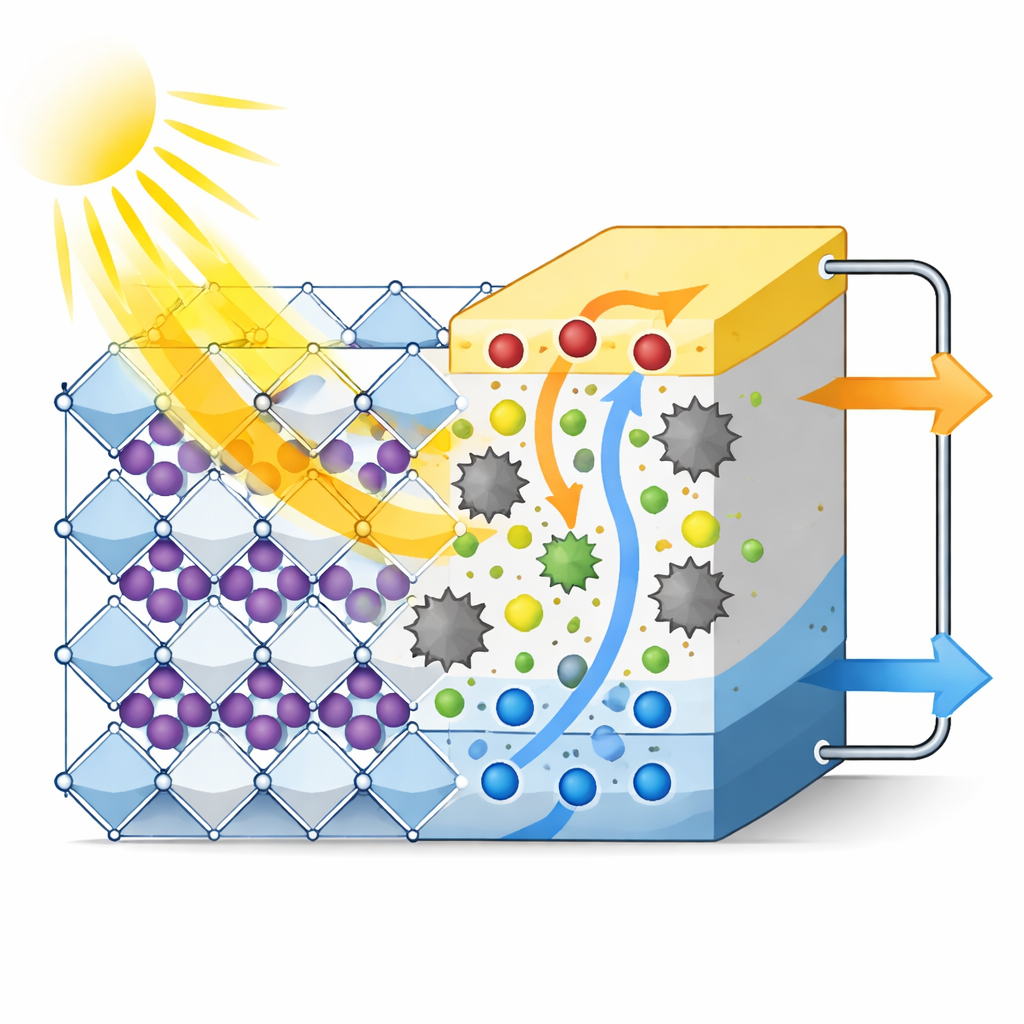
Why cleaner solar materials matter
Solar panels are often seen as a clean alternative to fossil fuels, but many of today’s highest‑efficiency solar cells rely on compounds that contain toxic lead and fragile organic components. This review article explores a new class of solar materials—fully inorganic, lead‑free perovskites—that aim to keep the impressive light‑harvesting ability of current devices while greatly improving safety and durability. For readers interested in the future of clean energy, it offers a big‑picture map of where the field is heading and what still stands in the way.

Building a sturdier solar crystal
Perovskites are a family of crystals whose structure is especially good at absorbing sunlight and moving electric charges. The best-performing versions so far use an organic molecule at one site in the lattice and lead at another. Unfortunately, the organic parts fall apart in heat, moisture, and strong light, while lead raises serious environmental and health concerns. Researchers therefore look to fully inorganic designs where the organic piece is replaced by cesium and the lead is swapped out for less toxic metals. The article compares several such families—based on tin and germanium, bismuth and antimony, and silver–bismuth “double” perovskites—and explains how small changes in crystal shape and bonding can make or break solar performance.
Swapping lead for tin and germanium
The closest electrical stand‑ins for lead are tin and germanium, which can form three‑dimensional perovskite frameworks that absorb visible light strongly and, on paper, can rival the best lead compounds. Tin‑based materials in particular can reach nearly ideal band gaps for solar energy conversion and can transport charges over micrometer distances, comparable to today’s commercial‑grade perovskites. The catch is that tin and germanium are much easier to oxidize. This chemical fragility spawns defects in the crystal that act like tiny pits, trapping charges and turning useful energy into heat. The review describes how careful control of composition, processing temperature, and the use of helper additives can slow down oxidation, smooth out film growth, and dramatically extend device lifetimes, bringing efficiencies above 14% for some tin-based cells.
Turning low‑dimensional crystals into better light harvesters
Bismuth- and antimony‑based perovskites take the opposite trade‑off: they are chemically robust and resistant to moisture, but their atoms link up in low‑dimensional clusters and sheets rather than in a fully connected three‑dimensional network. This geometry tends to trap charges in place and gives indirect band gaps, so light is not converted into electricity as efficiently. The authors show how changing the balance of ions, inserting smaller or larger cations, or partially replacing the halide ions can nudge these structures toward more connected arrangements with better charge mobility. Surface treatments and carefully tuned growth conditions further help by reducing deep defects that act as efficient “killers” of excited charges. Even so, efficiencies for these safer compounds remain modest, generally in the low‑single‑digit percentage range.
Designing double perovskites and taming defects
Another promising route replaces each pair of lead atoms with a combination of a +1 metal such as silver and a +3 metal such as bismuth, forming so‑called double perovskites. These materials are structurally stable and show surprisingly long lifetimes for excited charges, yet they usually possess relatively wide and often indirect band gaps, limiting how much sunlight they can harvest. The review highlights tactics to shrink and reshape these gaps—such as mixing in other metals, gently distorting the crystal with strain, or introducing controlled disorder in the metal arrangement. Across all families, one unifying message emerges: the way that atomic orbitals form the top and bottom of the energy bands largely dictates which defects appear, whether they are shallow and harmless or deep and highly destructive. Successful engineering strategies work by steering both the band edges and the defect landscape toward conditions where recombination losses are minimized.
From lab curiosity to real‑world power source
Looking ahead, the article argues that lead‑free inorganic perovskites could underpin a new generation of safer solar modules, including tandem devices that stack different absorbers to squeeze more energy from sunlight. To get there, scientists must still solve several intertwined problems: preventing oxidation of tin and germanium without sacrificing film quality, loosening the charge‑trapping tendencies of bismuth and antimony frameworks, carefully matching energy levels at interfaces, and developing scalable coating methods that yield uniform, defect‑poor films over large areas. With coordinated progress in crystal chemistry, processing, and long‑term testing under realistic conditions, these materials could deliver solar panels that are not only efficient, but also robust and environmentally responsible.
Citation: Jang, W.J., Park, P.J., Ong, WJ. et al. Stable and eco-friendly inorganic lead-free perovskite solar cells: structural, electronic, and defect engineering. Commun Mater 7, 110 (2026). https://doi.org/10.1038/s43246-026-01158-1
Keywords: lead-free perovskites, inorganic solar cells, tin-based perovskites, bismuth and antimony perovskites, double perovskite photovoltaics