Clear Sky Science · en
Morphotaxial Cu doping in monolayer MoS2 for high-performance optoelectronics
Turning Ultra-Thin Crystals into Better Light Sensors
Our phones, cameras, and future smart devices all rely on tiny components that can sense light quickly and accurately. Engineers are now exploring atomically thin materials—only a single layer of atoms thick—to shrink these light sensors even further. This paper shows how a clever chemical treatment can dramatically boost the performance of one such material, paving the way for faster, more sensitive, and more energy-efficient optoelectronic devices.
Why Flat Crystals Matter for Future Electronics
Two-dimensional materials, which are only one atom thick, have unusual electrical and optical properties that make them attractive for next‑generation electronics. One of the most studied examples is molybdenum disulfide (MoS2), a sheet of molybdenum atoms sandwiched between sulfur atoms. Because it absorbs and emits light efficiently, monolayer MoS2 is a strong candidate for tiny LEDs, solar cells, and especially photodetectors—devices that turn light into electrical signals. However, practical MoS2 photodetectors suffer from a serious problem: even in the dark they can carry a relatively large, noisy current, and after light is turned off they can stay “stuck on” for seconds to minutes due to trapped charges. This high dark current and slow relaxation limit how precisely they can detect faint or rapidly changing light signals.
A Gentle Way to Add Helpful Atoms
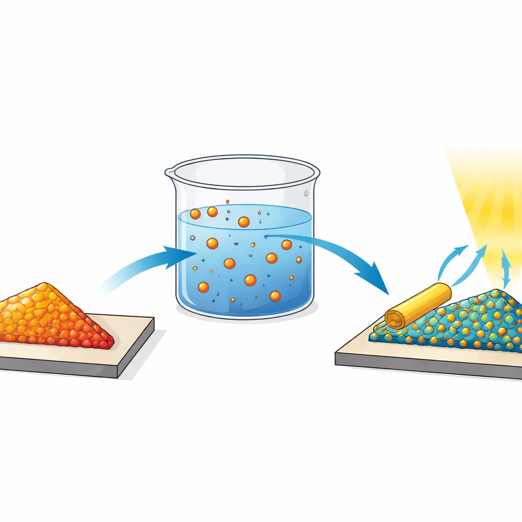
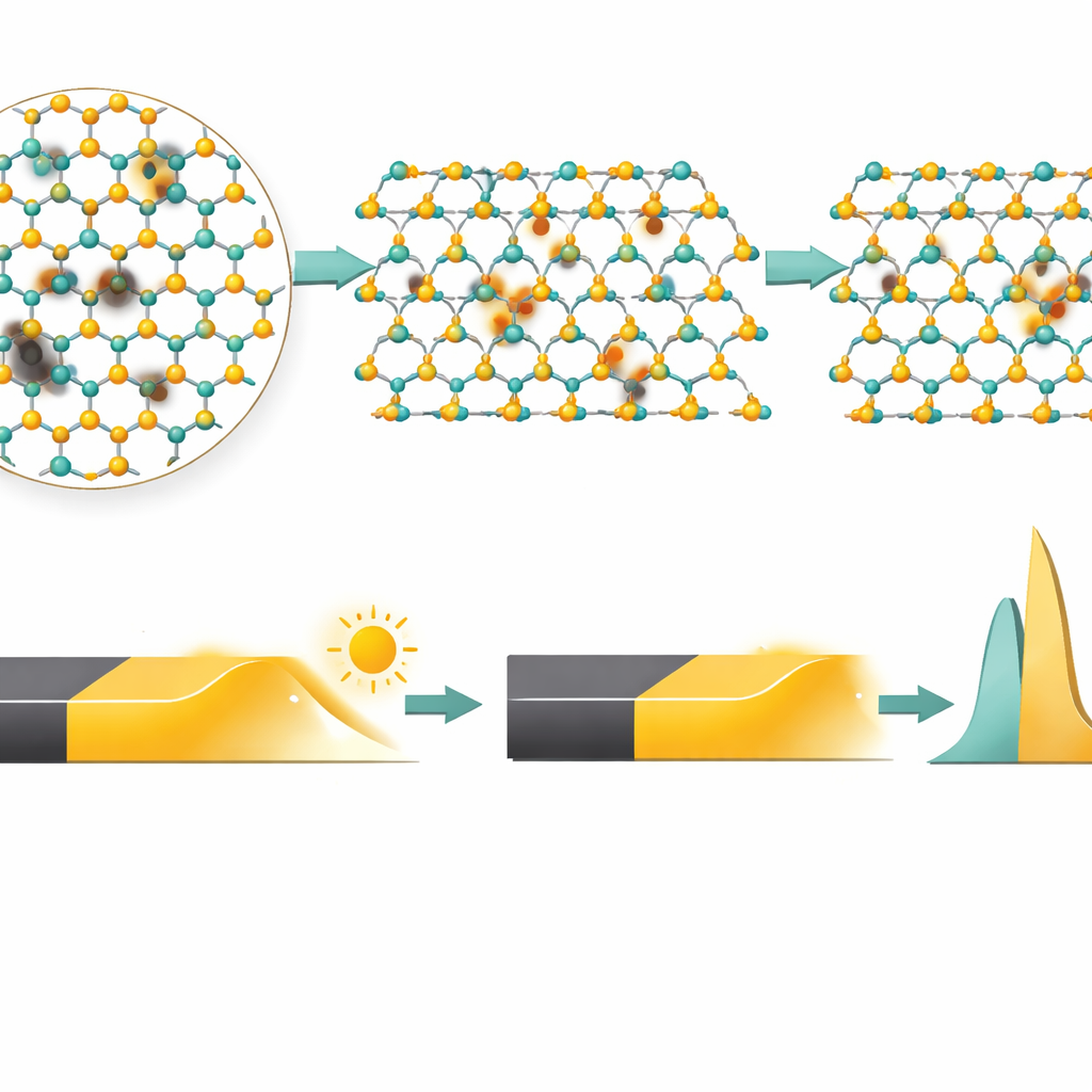
In conventional silicon chips, performance is tuned by “doping”—swapping a small fraction of atoms in the crystal with different elements that donate or accept electrons. But the usual method, firing energetic ions into the material, is too violent for fragile one‑atom‑thick layers. The authors instead use a process called morphotaxial cation exchange, a solvent-based treatment that lets copper (Cu) atoms quietly slip into the MoS2 lattice. Chemical vapor deposition first grows large, uniform MoS2 monolayers on a silicon oxide surface. These flakes are then immersed in a warm acetone solution containing a copper salt. During the reaction, some molybdenum atoms are replaced by copper, but the overall triangular shape and thickness of each flake are preserved—a key feature of morphotaxy, which keeps the original crystal outline intact while changing its internal composition.
Proving That Copper Really Changes the Crystal
The team uses a suite of microscope and spectroscopy techniques to confirm what happened inside the material. High-resolution electron microscopy shows individual copper atoms sitting where molybdenum atoms used to be, and elemental mapping reveals that copper is spread evenly across the flakes rather than clumping at the edges. Raman and photoluminescence measurements—both sensitive to how atoms vibrate and how electrons recombine—indicate that the material has shifted from its usual electron‑rich (n‑type) state toward a hole‑rich (p‑type) state when copper is introduced. X‑ray photoelectron spectroscopy and surface potential mapping further show that the material’s internal energy landscape has shifted so that its Fermi level moves closer to the valence band, consistent with p‑type doping. Together, these tests paint a consistent picture: a few percent of molybdenum atoms have been replaced by copper, subtly but decisively altering the electronic structure.
Quieter, Faster, and More Sensitive Light Detection
The real test is whether this atomic surgery improves device behavior. The researchers fabricate dozens of phototransistors before and after copper treatment, all with identical geometry, and carefully compare their performance. After doping, the dark current—the unwanted current flowing with no light—drops by about four orders of magnitude, from around billionths of an ampere to trillionths. At the same time, the ratio of light current to dark current rises from roughly 10–100 to about 10,000, meaning light signals stand out much more clearly against the background. Time-resolved measurements show that pristine MoS2 devices take tens of seconds to turn fully on and off because carriers get stuck in deep defect states. Copper-doped devices, in contrast, respond in a few hundred milliseconds. Analysis of the transient signals reveals that copper has effectively reshaped the “trap landscape,” shifting the dominant traps from slow, deep ones to faster, shallow ones and reducing the overall electrical noise. As a result, the detectors reach specific detectivity values up to about 10^14 Jones—a measure of how well they can spot weak light—placing them among the best reported devices based on this type of material.
What This Means for Everyday Technology
For non-specialists, the message is that a gentle chemical treatment can turn a promising but imperfect atom‑thin crystal into a far more practical light sensor. By swapping a small fraction of atoms for copper without damaging the material’s shape, the authors simultaneously cut dark current, speed up response times by more than a factor of ten, and lower noise. Because the method is solvent-based and compatible with standard chip processing, it could be scaled up to large areas. This approach shows that carefully chosen substitutional dopants can act not just as simple charge donors or acceptors, but as tools to tame defects and fine‑tune how ultrathin materials interact with light—an important step toward compact cameras, optical communication links, neuromorphic circuits, and other advanced technologies built from 2D semiconductors.
Citation: Rajput, M., Shukla, A., Mahapatra, A. et al. Morphotaxial Cu doping in monolayer MoS2 for high-performance optoelectronics. Commun Mater 7, 119 (2026). https://doi.org/10.1038/s43246-026-01120-1
Keywords: 2D materials, MoS2 photodetector, semiconductor doping, copper morphotaxy, optoelectronics