Clear Sky Science · en
Engineering in 2D violet phosphorus/PdSe2 van der Waals heterostructures for advanced optoelectronics
Why this tiny light sensor matters
From phone cameras to fiber‑optic cables, modern life depends on devices that can sense light quickly and efficiently. This article explores a new kind of ultrathin light sensor built from stacked sheets of crystalline materials only a few atoms thick. By carefully arranging these layers and adding a sheet of graphene as a smart contact, the researchers create a photodetector that is not only highly sensitive and fast, but can also distinguish the direction in which light is polarized. Such devices could help power future wearable electronics, imaging systems, and optical communication links that are smaller, cooler, and more energy‑efficient than today’s technology.
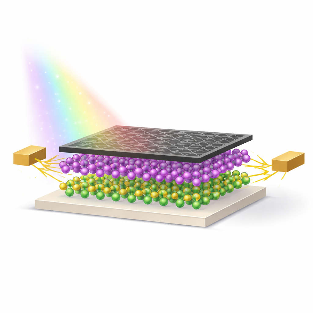
Building with ultra‑thin Lego bricks
The heart of the work lies in so‑called two‑dimensional materials, crystals that can be peeled down to layers only a few atoms thick. When such layers are stacked, they touch through gentle van der Waals forces rather than conventional chemical bonds, forming clean, atomically sharp junctions. The team combines two such materials: violet phosphorus, which has strongly directional optical behavior, and palladium diselenide, a transition‑metal compound known for its wide tuning range and high charge mobility. By placing one atop the other, they create a van der Waals heterostructure designed to harvest light across the visible to near‑infrared range, roughly from 405 to 808 nanometers.
Designing the energy landscape
To understand how this stack will behave before fabricating devices, the authors use quantum‑level computer simulations. These calculations show that when violet phosphorus and palladium diselenide are combined, their electronic energy levels line up in what physicists call a type‑I configuration. In simple terms, both negative and positive charge carriers prefer to sit in the palladium diselenide layer, which acts like a shallow well. The simulations also reveal charge rearrangement at the interface and an internal electric field strong enough to keep carriers from easily escaping. This arrangement favors efficient light emission and absorption, and it sets the stage for strong electrical signals when the structure is used as a photodetector.
From theory to working devices
The researchers then build actual devices by mechanically exfoliating thin flakes of the two materials and stacking them on a silicon chip. Microscopy confirms that the layers are just a few nanometers thick and uniformly joined, while optical probes such as Raman scattering and photoluminescence mapping show that the interface is clean and active. When contacted with metal electrodes and tested under light, the basic violet phosphorus/palladium diselenide diode responds to several wavelengths, with particularly strong performance at green light where both layers absorb efficiently. Even at very low light levels, the device generates a measurable current, demonstrating its promise as a sensitive detector.
Giving the detector a graphene boost
To push performance further, the team adds a thin layer of graphene on top of the violet phosphorus side as a specially engineered contact. Graphene is both highly conductive and nearly transparent, making it an ideal bridge for extracting photo‑generated charges without blocking incoming light. This simple addition transforms the device: the electrical response to light jumps by roughly three orders of magnitude, reaching a responsivity of about 111 amperes per watt and an external quantum efficiency exceeding 26,000 percent under green illumination. At the same time, the response speed tightens to around ten milliseconds, more than ten times faster than the version without graphene. Measurements of the surface potential show that graphene sharpens the built‑in electric field at the junction, improving carrier separation and transport while also shielding the more delicate violet phosphorus from environmental damage.
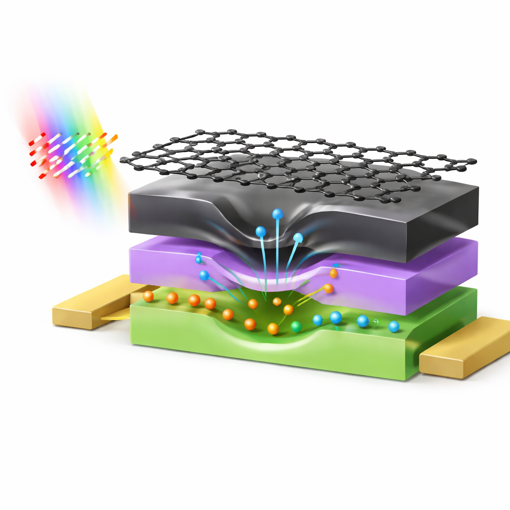
Seeing the direction of light
Beyond simple brightness, the enhanced detector can also sense the orientation of light waves. Because both violet phosphorus and palladium diselenide interact differently with light depending on direction within the crystal plane, the device’s output rises and falls as the polarization angle of the incoming beam is rotated. Tests across three wavelengths reveal a clear oscillating response and elliptical polar plots, signatures of strong polarization sensitivity. While adding graphene slightly softens the contrast compared with the bare stack, it preserves robust directional behavior while greatly improving speed, stability, and overall signal strength. The device remains stable over at least one hundred on‑off cycles at multiple colors, underscoring its durability.
What this means for future gadgets
In essence, the authors show that careful “contact engineering” in ultrathin material stacks can turn a good light sensor into an exceptional one. By combining a favorable energy arrangement in the violet phosphorus/palladium diselenide pair with a graphene contact that eases charge flow and protects the structure, they achieve a compact photodetector that is fast, highly responsive, and able to read polarization over a broad range of colors. Such multifunctional, stable devices made from only a few atomic layers could become key building blocks in future imaging chips, compact optical links, and wearable sensors where high performance and low power consumption are both essential.
Citation: Ahmad, W., Rehman, M.U., Zhuang, Q. et al. Engineering in 2D violet phosphorus/PdSe2 van der Waals heterostructures for advanced optoelectronics. Commun Mater 7, 102 (2026). https://doi.org/10.1038/s43246-026-01114-z
Keywords: 2D photodetectors, van der Waals heterostructures, graphene contacts, violet phosphorus, polarization-sensitive imaging