Clear Sky Science · en
Confinement epitaxy of large-area two-dimensional Sn at the graphene-SiC interface
A New Way to Tame Graphene
Graphene—an atom-thin sheet of carbon—is famous for being incredibly strong, conductive, and versatile. But in real devices, it usually sits on a supporting crystal and sticks to it in ways that spoil some of its best properties. This paper explores a clever workaround: sliding a single-atom-thick layer of tin between graphene and its silicon carbide base. The result is a more “free” graphene layer and a buried metallic sheet that can be used to tune strain and electronic behavior, pointing toward smarter platforms for future quantum and electronic technologies. 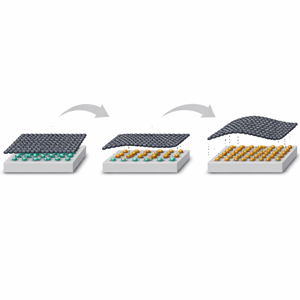
Building a Hidden Metal Sandwich
The work starts from a special form of graphene on silicon carbide known as a “zero-layer,” where the carbon honeycomb is partially bonded to the crystal beneath and behaves more like an insulator than a metal. The researchers deposit tin atoms on top and then heat the sample so that tin moves under the graphene instead of sitting on top. This “intercalation” process is guided by the graphene layer itself, which acts like a rigid, chemically inert lid that confines the tin to a flat, two-dimensional sheet at the buried interface. Careful electron diffraction measurements show that the tin does not clump into islands; instead, at full coverage it forms a well-ordered triangular lattice locked to the silicon carbide surface, while the graphene above largely lets go of its chemical bonds to the substrate and becomes quasi-free-standing.
Letting Atoms Sneak In from the Side
To understand how this hidden layer forms and how to keep the graphene in good shape, the team compares two pathways: direct tin deposition onto exposed areas of the surface and lateral diffusion of tin underneath a shadow mask. Raman microscopy, which tracks subtle shifts in the vibrations of the carbon lattice, reveals that regions filled by sideways diffusion contain far fewer defects and more uniform graphene than regions exposed directly. The diffusion front advances tens of micrometers under the mask, producing a smoother interface and larger defect-free patches of graphene. This suggests that controlling how tin spreads—not just how much is deposited—is key to maintaining high crystalline quality and avoiding damage during processing. 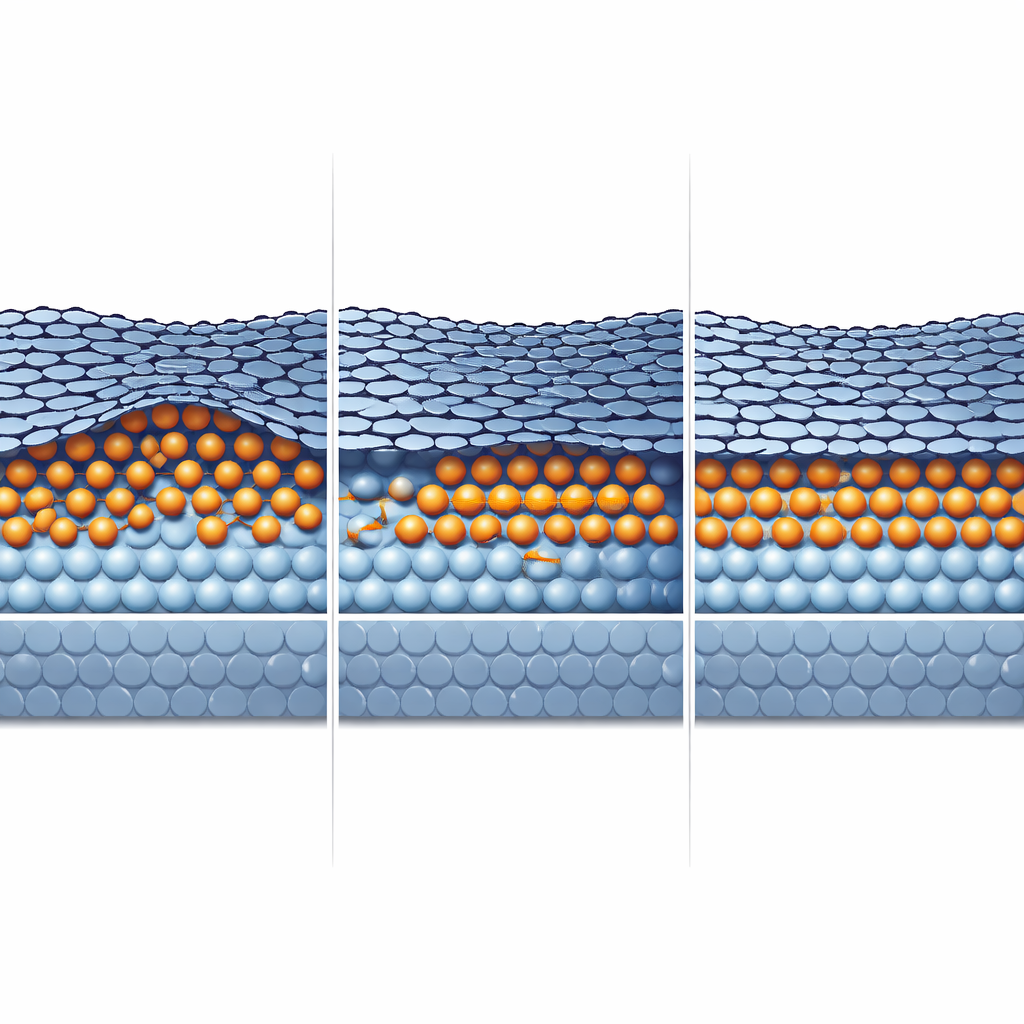
Stretching and Calming the Carbon Sheet
The buried tin layer does more than simply hold graphene up. Because tin and silicon carbide expand differently with temperature than graphene does, heating and cooling the stack introduce tiny but measurable strains in the carbon sheet. By monitoring how characteristic graphene Raman peaks shift with temperature, the authors show that the metallic tin layer acts like a built-in “stress amplifier,” enhancing how strongly graphene responds to heating while still keeping its structure stable. At low temperatures, the negative thermal expansion of graphene can even balance the expansion of the substrate-plus-tin stack, creating a plateau in the vibrational response. This dynamic interplay between layers demonstrates that strain in graphene can be tuned not only by bending or stretching from the outside, but also by engineering what lies invisibly beneath it.
Restoring Neutral, Clean Graphene
Using angle-resolved photoemission spectroscopy, the researchers directly visualize the electronic bands of the system. They find a sharp Dirac cone—the hallmark of high-quality graphene—with its crossing point essentially at the Fermi level, meaning the graphene is nearly perfectly charge neutral. This is surprising because the underlying silicon carbide crystal usually pulls charges out of nearby materials. The intercalated tin layer behaves as a metallic screen, cancelling the built-in electric fields and preventing unwanted doping of the graphene. At the same time, the tin itself shows a clear metallic band structure and remains stable even after exposure to air, protected by the graphene lid. Only at very high temperatures does tin begin to escape or react with the substrate, underlining both the robustness and limits of this confined architecture.
Why This Matters for Future Devices
Putting it all together, the study shows that a single-atom-thick tin layer, trapped between graphene and silicon carbide, can simultaneously free graphene from the substrate, keep it charge neutral, and offer a new handle to tune strain and coupling through temperature and structure. Because the process works over large areas and relies on a general “confinement epitaxy” concept—growing materials in the narrow space beneath a two-dimensional lid—it can be extended to other metals and 2D materials. For non-specialists, the takeaway is that the authors have developed a way to hide a controllable, durable metal layer under graphene without spoiling its surface, opening new routes toward stable, tunable platforms for quantum electronics, sensing, and advanced photonic devices.
Citation: Mamiyev, Z., Tilgner, N., Balayeva, N.O. et al. Confinement epitaxy of large-area two-dimensional Sn at the graphene-SiC interface. npj 2D Mater Appl 10, 51 (2026). https://doi.org/10.1038/s41699-026-00700-6
Keywords: graphene, two-dimensional tin, intercalation, strain engineering, graphene–metal heterostructures