Clear Sky Science · en
2D materials assisted terahertz modulators and sensors
Why tiny sheets of matter can reshape wireless and sensing
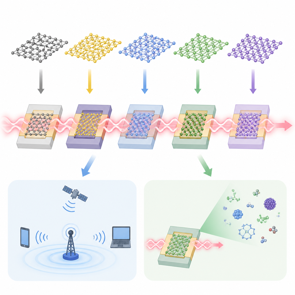
Smartphones, airport scanners, and even medical tests all rely on waves that carry information. Terahertz waves, which sit between microwaves and infrared light, promise faster short-range wireless links and gentle, non-destructive scanning of food, artwork, and living tissue. Yet today, our tools for steering and detecting these waves are bulky, power-hungry, and often too slow. This article explores how ultra-thin "two-dimensional" materials made of just a few atomic layers could unlock nimble terahertz devices that fit on a chip, opening new options for communication and sensing.
What makes terahertz waves special
Terahertz waves occupy a slice of the spectrum that can pass through many non-metallic materials while carrying subtle signatures of the molecules they touch. They can reveal vibrations and rotations of chemicals in food, pollutants in water, or structural details hidden inside paintings and packaging. However, making practical systems has been hard because we lack efficient parts that can quickly turn terahertz beams on and off, change their strength or phase, or read tiny changes caused by molecules on a surface. Traditional silicon and metal parts suffer from low carrier mobility, narrow operating ranges, high drive voltages, and slow response, which limits both communication speeds and sensing accuracy.
Why flat materials offer new control
Two-dimensional materials such as graphene, transition metal dichalcogenides, black phosphorus, porous frameworks, and MXenes consist of one or only a few atomic layers. Their extreme thinness means most atoms sit at the surface, making them very sensitive to electric fields, strain, light, and nearby molecules. In graphene, electrons move with very high mobility and no natural bandgap, so its electrical and optical response at terahertz frequencies can be tuned smoothly with a small gate voltage or chemical doping. Other 2D materials offer adjustable bandgaps, strong light absorption, or built-in electric polarization, which can all be harnessed to reshape passing terahertz waves. Stacking different 2D layers without the usual crystal matching rules allows designers to build custom "van der Waals" structures tailored for specific tasks.
New ways to modulate terahertz signals
By combining these thin materials with patterned metal structures called metasurfaces, researchers have built a family of compact terahertz modulators. Electrical devices adjust the carrier density in graphene or related sheets, changing how strongly they absorb or reflect a terahertz beam; some achieve almost total on–off contrast with only a few volts. Optical modulators shine a separate laser to create carriers in a 2D layer or its substrate, switching terahertz transmission within trillionths of a second. Magnetic approaches use strong fields to twist the polarization of terahertz waves in graphene, enabling non-reciprocal elements like isolators. Together, these methods cover high modulation depth, fast speed, and broad bandwidth, key ingredients for future high-capacity wireless links.
Turning flat materials into sensitive noses
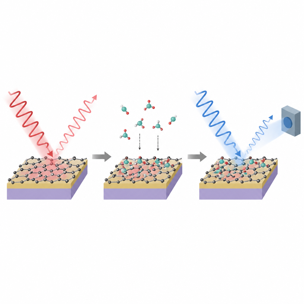
When pesticide molecules, antibiotics, strands of DNA, proteins, or even viruses land on a 2D surface, they slightly change its charge and bonding environment. At terahertz frequencies, this alters how the material absorbs or delays the wave. By placing 2D layers on carefully designed resonant structures, very small shifts in the resonance frequency, amplitude, or phase can be measured. Experiments have detected pesticide residues on fruit peels, antibiotics at nanogram levels, and specific DNA sequences and plant proteins at tiny concentrations, all without fluorescent labels. Hybrid designs using MXenes or porous frameworks exploit high surface area and tunable pores to further boost sensitivity, while flexible substrates allow sensors that bend with wearables or curved packages.
Promise, obstacles, and where this is heading
The article concludes that atomically thin materials can outperform bulk silicon and metals in many terahertz tasks, combining low power use, high speed, and the ability to integrate sensing and modulation on small chips. Still, there are hurdles: some materials degrade in air or under light, large-area growth and precise stacking remain difficult, and the very short thickness of the active layers demands clever structures to keep strong interaction with terahertz waves over a broad range of frequencies. The authors argue that progress in material chemistry, device engineering, and compact terahertz sources will be needed to move from lab prototypes to everyday tools. If achieved, 2D-material-based terahertz components could underpin future secure wireless networks, rapid quality checks in industry, and gentle, label-free medical diagnostics.
Citation: Wang, H., Bao, Y., Wang, B. et al. 2D materials assisted terahertz modulators and sensors. npj 2D Mater Appl 10, 56 (2026). https://doi.org/10.1038/s41699-026-00687-0
Keywords: terahertz technology, 2D materials, graphene sensors, metasurfaces, wireless communication