Clear Sky Science · en
Dual carrier-selective contact transition metal dichalcogenide solar cells
Making Power from Ultra-Thin Materials
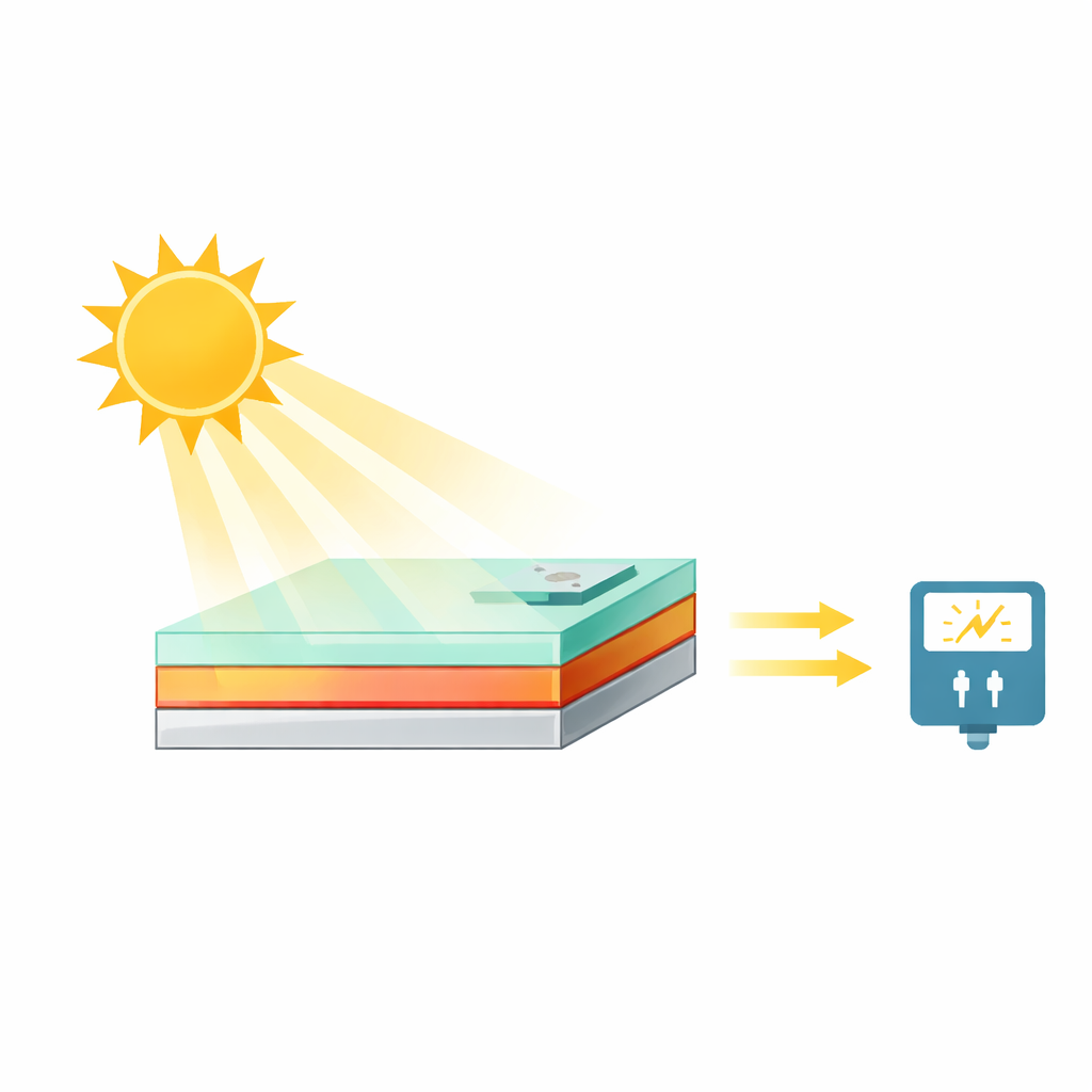
Imagine a solar panel so thin it is almost transparent, yet it still grabs sunlight with surprising strength. This study explores how sheets of special crystals only billionths of a meter thick can be turned into lightweight, high-power solar cells. The researchers show a new way of wiring these ultrathin materials so that they waste less energy, a step that could help future solar panels power satellites, electric vehicles, and portable electronics where every gram and every watt matters.
Why New Solar Layers Are Needed
Most current solar cells are made from relatively thick slabs of silicon or other semiconductors. In contrast, transition metal dichalcogenides (TMDs) such as WS2 can absorb visible light extremely well even when they are only a few nanometers thick. That makes them attractive for applications where low weight and flexibility are crucial. However, when these ultrathin crystals are placed directly against metal electrodes, many of the generated charges simply recombine and vanish as heat at the interface. Effects such as poor energy alignment and unwanted pathways for current drastically reduce the voltage and efficiency compared with what simple theory predicts.
A Sandwich Design that Guides Charges
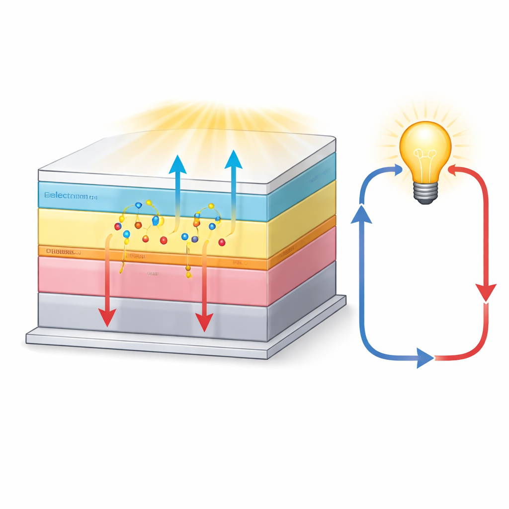
To fix this, the team borrowed ideas from high‑performance silicon and perovskite solar cells, which use “carrier‑selective contacts” that guide only one type of electrical charge. They built a vertical stack just 10 nanometers thick in the active region: an ultrathin WS2 layer in the middle, a hole‑selective organic layer called PTAA beneath it, and an electron‑selective fullerene layer (C60) on top, capped with metal electrodes. Light is absorbed in the WS2 layer, and the selective contacts are engineered so that electrons are drawn upward into the C60 and holes are drawn downward into the PTAA, while unwanted recombination at the metal interfaces is strongly suppressed.
Tuning the Layers for Smooth Power Flow
In early versions of the device, the electrical output curve bent into an S‑shape, a sign that one side of the cell was acting like a bottleneck. Simulations and experiments showed that the electron‑selective C60 layer was less conductive than the PTAA layer, causing charge build‑up and energy loss. By thinning the C60 layer from 20 nanometers to just 2 nanometers, the researchers greatly improved the balance between the two contacts. The final devices reached an open‑circuit voltage of 523 millivolts, a fill factor of 0.54, and a power conversion efficiency of 2.4% under standard sunlight for a WS2 sheet only 10 nanometers thick.
Looking Inside How Charges Travel
Using finely focused laser beams, the team mapped how current spreads across the device. They found that charges generated far from the metal contact could still be collected, indicating that electrons travel on average about 13 micrometers before recombining—remarkably long compared with the thickness of the absorber. Additional measurements revealed that minority charges in WS2 persist for about 100 picoseconds, while device behavior hinted that majority charges effectively live much longer because they are efficiently extracted by the selective contacts. This combination of long travel distance and guided extraction helps the ultrathin device harvest a large fraction of the light it absorbs.
What Limits the Voltage and How to Improve It
The researchers then asked how close their devices are to the ultimate performance allowed by the material itself. By combining optical models with simple lifetime‑based formulas, they showed that the short time that charges survive in multilayer TMDs is a key factor limiting the voltage. For a 10‑nanometer‑thick WS2 layer with a 100‑picosecond lifetime, the theoretical voltage limit is about 663 millivolts—only about 140 millivolts higher than what they already achieved. To push beyond this, they suggest improving the purity and structure of the TMD layers to extend carrier lifetimes into the microsecond range, and further refining the contact materials so that their energy levels and conductivities are better matched to WS2 or related TMDs such as WSe2.
Path Toward Practical Ultra-Light Solar Cells
In simple terms, this work shows that carefully tailored “one‑way doors” for positive and negative charges can unlock much better performance from ultrathin solar materials. The new dual‑contact WS2 cell already delivers respectable voltage and efficiency for such a thin absorber, and the underlying design principles can be applied to other TMDs and large‑area manufacturing methods. With longer‑lived charges, improved contacts, and optimized light‑trapping structures, these featherweight solar cells could one day rival conventional panels while offering far higher power per unit weight for space missions, vehicles, and wearable electronics.
Citation: Went, C.M., Tham, R.W., Jahelka, P.R. et al. Dual carrier-selective contact transition metal dichalcogenide solar cells. npj 2D Mater Appl 10, 50 (2026). https://doi.org/10.1038/s41699-026-00684-3
Keywords: ultrathin solar cells, transition metal dichalcogenides, carrier-selective contacts, WS2 photovoltaics, high-specific-power energy