Clear Sky Science · en
Grain-boundary-driven stochastic oxide junction in 2D SnSe enables dual electrical-optical PUFs
Why tiny flaws can protect your digital life
Modern gadgets—from smart locks to connected cars—rely on secret codes that can sometimes be copied or hacked. This study shows how the natural imperfections inside an ultrathin crystal film of tin selenide (SnSe) can be turned into a built‑in, unclonable “fingerprint” for each chip. By gently rusting parts of the film in a controlled way, the researchers create a complex, random pattern that can be read electrically and optically, offering a new route to secure, tamper‑resistant hardware without intricate chip designs.
Turning a flat film into a maze
The work begins with smooth, large‑area films of a two‑dimensional semiconductor, SnSe, grown from a solution on silicon wafers. Though the surface looks uniform, the film is actually made of many tiny crystal grains stitched together by grain boundaries—thin internal seams where atoms do not line up perfectly. These hidden seams become the key to the security scheme. The team exposes the films to ultraviolet light in an oxygen‑rich environment, a process that encourages oxygen atoms to slip into the SnSe along the grain boundaries. Over time, these regions partially convert into tin dioxide (SnO₂), an insulating oxide, while the spaces between them remain mostly SnSe. The once even layer is transformed into an intricate mosaic of conducting and insulating zones that no conventional lithography tool ever draws.
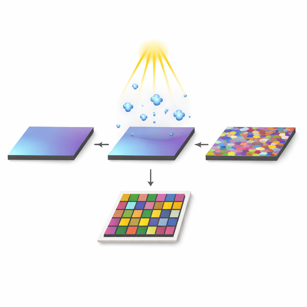
Watching the film quietly rearrange itself
To see what this hidden rearrangement looks like, the researchers use powerful microscopes and surface‑sensitive probes. Electron microscopy shows that the original SnSe films are well‑ordered and chemically uniform: tin and selenium are spread evenly, and the film is only about 20 nanometers thick—thousands of times thinner than a human hair. After controlled UV treatment, the picture changes. Atomic‑force microscopy reveals a rougher, grain‑textured surface, and chemical maps show oxygen concentrating along specific lines that match the grain boundaries. X‑ray measurements track tin atoms shifting from a lower to a higher oxidation state, confirming the gradual birth of SnO₂ regions inside the SnSe matrix. At the same time, the films absorb less visible light and their electrical sheet resistance becomes more irregular across the surface, clear signs that the internal landscape has become patchy and varied.
From random paths to secret digital keys
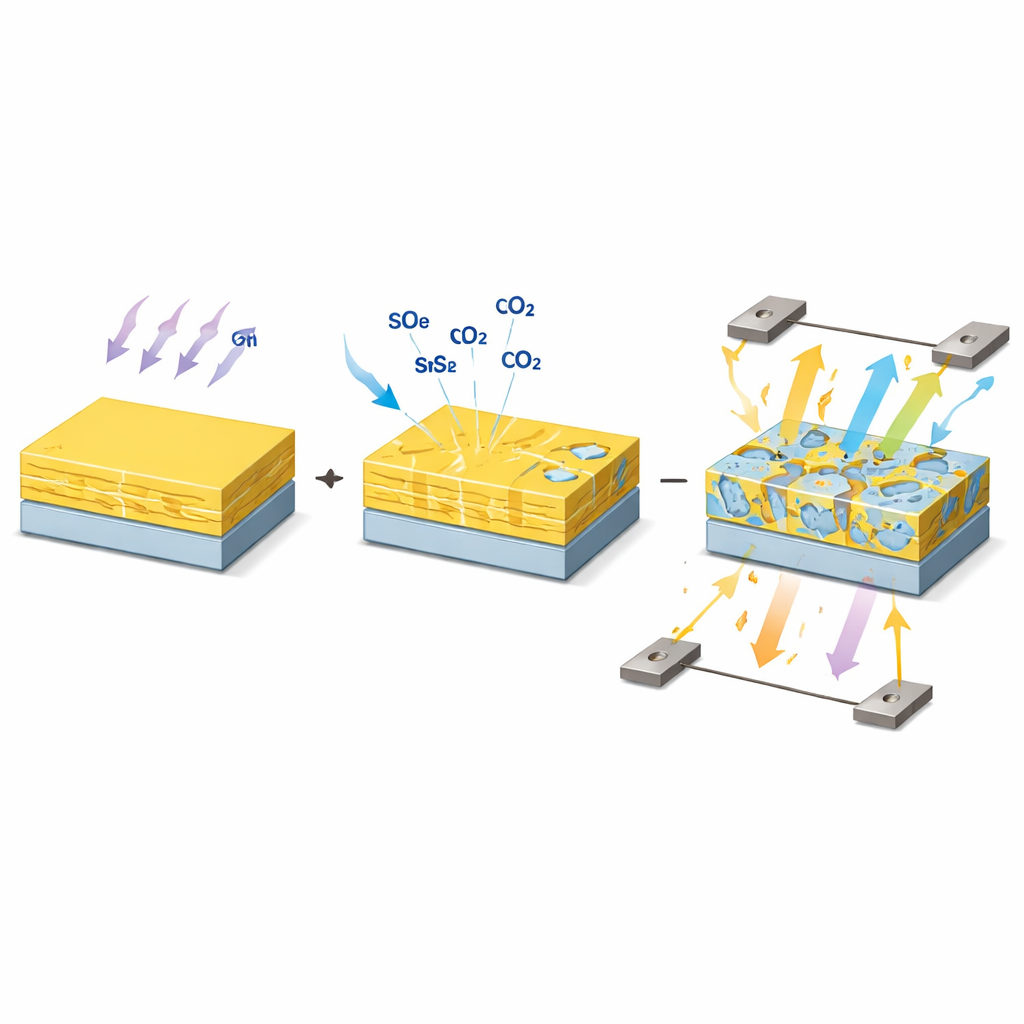
These microscopic changes strongly affect how current flows through devices built from the films. The team fabricates 15 × 15 arrays of tiny diodes by stacking the SnSe layer between a silicon wafer and metal contacts. Before oxidation, the devices behave similarly: their current–voltage curves line up closely, and the array is fairly uniform. After a short UV treatment, however, each diode sees a different local mix of SnSe and SnO₂ at its junction. Some paths become easier for electrons; others are partially blocked. The result is a broad spread of currents—spanning more than four orders of magnitude after longer oxidation—when the same voltage is applied across the array. By choosing an intermediate oxidation time, the researchers hit a sweet spot where the spread is large but the devices still work reliably. This diversity is exactly what is needed to turn the array into a physically unclonable function (PUF): each device location yields a slightly different analog current that can be converted into a unique pattern of digital zeros and ones.
Adding light as a second secret channel
The same film can also respond to light, providing a second, independent source of randomness. When the array is illuminated with gentle green light while a constant voltage is applied, extra charge carriers are generated in the mixed SnSe/SnO₂ junctions. Because each junction’s structure is slightly different, the light‑induced current changes vary from device to device in a way that does not simply mirror the dark behavior. The team measures current maps under several voltages, first in the dark and then under illumination, and turns each map into a binary key by comparing the current at each diode to a preset threshold. Statistical tests show that both electrical and light‑assisted keys have nearly perfect balance between zeros and ones and high randomness; importantly, the two modes are only weakly correlated. In other words, shining light on the same physical array effectively unlocks a second, orthogonal key space without changing the hardware.
Stable fingerprints for future secure hardware
For any security technology, stability is crucial. The researchers track selected devices for weeks in air, cycle the voltages hundreds of times, heat the samples, and subject them to accelerated aging. Across these tests, the current levels shift only slightly and, more importantly, preserve their relative ordering, so the derived digital keys remain consistent. The study concludes that a simple, uniform post‑treatment step—UV‑driven oxidation of a solution‑processed 2D SnSe film—can turn an otherwise ordinary semiconductor layer into a robust, reconfigurable source of physical randomness. Because the randomness is tied to the film’s intrinsic grain structure and oxide formation rather than to deliberate micro‑patterning, it should be extremely hard to copy, offering a promising path toward scalable, built‑in hardware fingerprints for the Internet of Things and beyond.
Citation: Song, J., Lee, D., Cho, J. et al. Grain-boundary-driven stochastic oxide junction in 2D SnSe enables dual electrical-optical PUFs. npj 2D Mater Appl 10, 52 (2026). https://doi.org/10.1038/s41699-026-00683-4
Keywords: hardware security, physical unclonable function, 2D materials, tin selenide, grain boundary oxidation