Clear Sky Science · en
AI-driven image processing framework for high-accuracy detection and characterization of vacancies in 2D materials
Why tiny gaps in ultra-thin materials matter
From flexible phones to ultrasensitive sensors and quantum devices, many future technologies rely on ultra-thin “sheet” materials just one atom thick. But these delicate layers are rarely perfect: they are peppered with tiny gaps where atoms are missing. These invisible pinholes can make or break a device’s performance. The paper behind this summary introduces a new artificial intelligence (AI) method that can spot and measure such gaps quickly and cheaply from ordinary images, potentially speeding up the design of better electronics and quantum materials.
Super-thin materials with super-sized potential
Materials like graphene, phosphorene, and molybdenum disulfide are famous for their remarkable strength, conductivity, and light-handling abilities, all squeezed into a layer just one atom thick. Engineers hope to use them in nanoelectronics, photonics, and quantum technologies. Yet their properties are extremely sensitive to flaws. Missing atoms, called vacancies, can weaken a device or, if carefully controlled, can create useful effects such as new electronic states or sensing sites. To harness these defects rather than be harmed by them, researchers must know exactly where the vacancies are, how big they are, and how many occur in a given area.
The problem with today’s close-up tools
Conventional ways to study these tiny gaps involve either powerful microscopes that can see individual atoms or heavy computer simulations that model every atomic motion. Techniques like transmission electron microscopy and molecular dynamics can be highly accurate, but they are slow, expensive, and difficult to scale to thousands of samples. Even newer vibration-based methods that infer defects from how a sheet shakes top out at around 90% accuracy and still need complex physical models. As the library of two-dimensional materials grows, these limitations become a serious bottleneck for discovering and optimizing new devices.
Teaching AI to read patterns in grayscale images
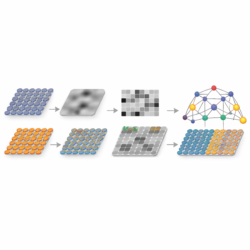
The author proposes an AI framework that skips atom-by-atom inspection and instead learns from patterns in simple grayscale images. First, realistic images of three types of 2D sheets are generated, each containing randomly placed circular holes of different sizes. These pictures are converted to black-and-white intensity maps, where the holes appear as brighter regions. Rather than feeding every pixel directly into a neural network, the method compresses each image into a carefully chosen set of 25 numerical features. These features capture how brightness is distributed across rows and columns, the shape and compactness of each hole, and overall image texture. They are designed so that a vacancy leaves a clear “signature” in these numbers.
How the machine learns to find missing atoms
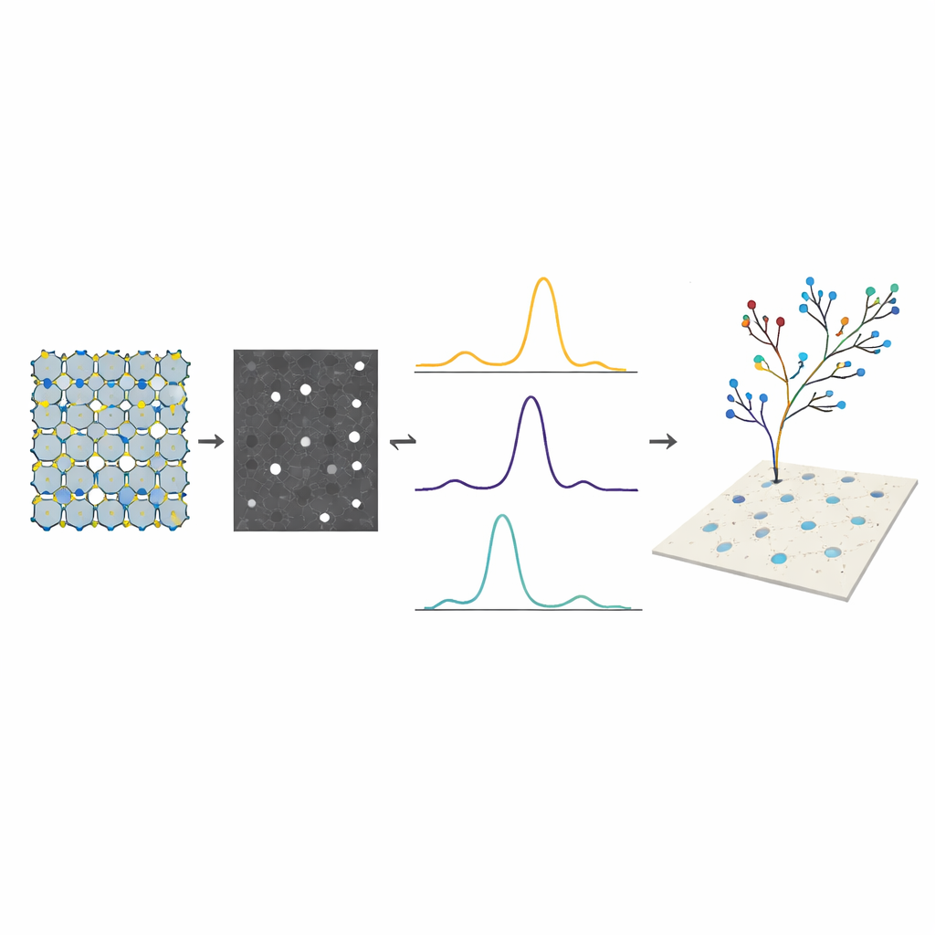
With thousands of simulated images and their known hole positions and sizes as training data, several machine learning models are tested. A tree-based method called a random forest emerges as the best balance between accuracy, speed, and interpretability. It learns to convert the 25 features into precise predictions of each hole’s horizontal and vertical position and its effective radius. For graphene, the trained model reaches test accuracies above 96%, with especially strong performance for the hole size. A statistical tool called SHAP is used to probe which features matter most, revealing, for example, that the average location of the strongest brightness peak is crucial for pinpointing the vertical coordinate. The approach also works when there are multiple vacancies in the same sheet: the image is segmented and each region analyzed in turn, with predicted hole sizes and densities closely matching the true values.
From simulation to real-world materials
Because the framework operates on standard grayscale images, it can in principle be applied to pictures from common microscopes without demanding specialized setups. It is also general enough to handle different lattice patterns, as shown by tests on graphene, phosphorene, and molybdenum disulfide. The method dramatically cuts both experimental and computational costs compared with traditional techniques, while providing detailed, numeric information rather than just “defect present or not.” Although this study mainly relies on simulated data, it outlines a path toward building shared experimental image databases and using the model as a community tool.
What this means for future devices
In plain terms, this work shows that a smart combination of image processing and machine learning can act like an automated inspector for atom-thin materials, spotting and sizing tiny gaps with high confidence. By turning simple images into rich numerical descriptions and then letting an AI model interpret them, researchers gain a fast, non-destructive way to map defects across many samples. This could accelerate the tuning of vacancies to improve conductivity, strength, or quantum behavior, helping push next-generation nanoelectronics and quantum technologies from the lab toward everyday use.
Citation: Alibagheri, E. AI-driven image processing framework for high-accuracy detection and characterization of vacancies in 2D materials. npj 2D Mater Appl 10, 44 (2026). https://doi.org/10.1038/s41699-026-00667-4
Keywords: 2D materials, vacancy detection, machine learning, image analysis, graphene