Clear Sky Science · en
Machine learning prediction of dual absorber lead-free perovskite solar cells for boosting PCE
Cleaner solar power for everyday life
Solar panels promise cheap, clean electricity, but many of today’s most efficient next generation designs rely on lead, raising concerns about toxicity and long term stability. This study explores a safer route by designing a lead free solar cell that still captures sunlight very efficiently, and it shows how computer simulations and machine learning can work together to guide future devices you might one day see on rooftops or in portable chargers.
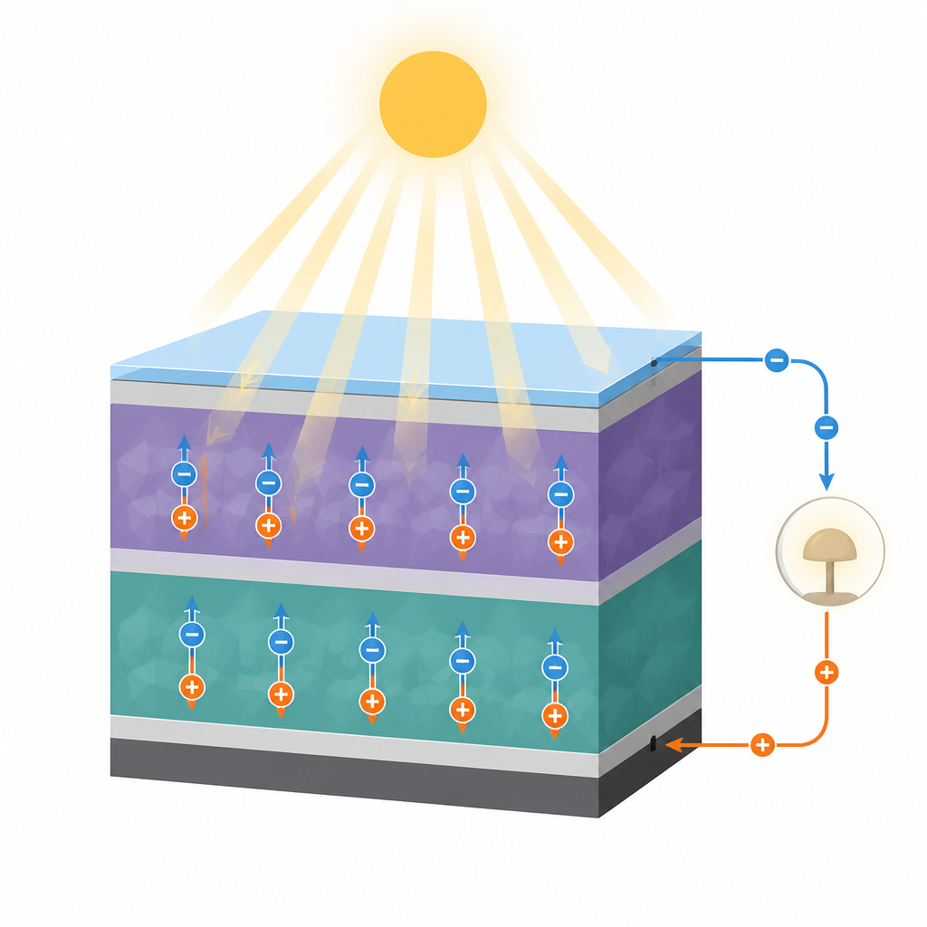
Two light catching layers working as a team
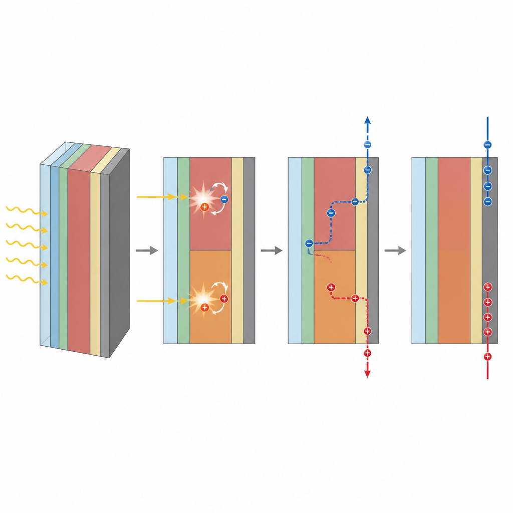
The researchers focus on a special class of materials called lead free double perovskites, which can be tuned to absorb different colors of sunlight while avoiding toxic elements. Instead of using a single light absorbing film, they stack two absorber layers: a top layer that prefers higher energy (bluer) light and a bottom layer that soaks up lower energy (redder) light that passes through. This “half tandem” or dual absorber design lets the cell harvest a broader slice of the solar spectrum without the complex wiring and current matching required in full tandem solar panels.
Building a high performance lead free stack
To design the device, the team uses a widely adopted solar cell simulator to test many virtual structures. The best performing layout sandwiches the dual absorber between carefully chosen charge transport layers that act like one way streets for electric charges. On the sun facing side, a layer of SnS2 guides electrons while blocking holes. On the rear side, a layer of Sb2S3 does the opposite, collecting holes and blocking electrons. The top absorber, made of Cs2TiCl6, has a wider bandgap and sits above a narrower bandgap Cs2AgBiI6 layer, so light is peeled off in stages as it travels through the stack. Gold or other high work function metals form the back contact, helping charges leave the device efficiently.
Tuning thickness, defects, and doping
The study shows that small details inside the layers strongly affect how well the cell works. If the top absorber is made too thick, it blocks light from reaching the bottom absorber and the current drops. If either absorber contains many defects, charges recombine before they can be collected, wasting energy. The simulations reveal sweet spots: a thin but high quality Cs2TiCl6 layer of about 100 nanometers above a thicker, low defect Cs2AgBiI6 layer around 1000 nanometers. Adjusting the number of charged atoms (doping) in each absorber and at the interfaces creates an internal electric field that helps pull electrons and holes apart. When bulk and interface defects are kept low and the doping is well tuned, the virtual device reaches a power conversion efficiency of about 32.7 percent, higher than comparable single layer versions of the same materials.
Letting algorithms sift through design choices
Exploring every possible combination of thickness, defect level, and doping by hand would be slow and inefficient. To speed this up, the authors feed more than two thousand simulated cases into several machine learning models. These models learn how changes in the physical parameters influence key solar cell outputs such as efficiency, voltage, current, and fill factor. Among the tested options, an approach called extreme gradient boosting gives the most accurate predictions, closely matching the simulator results. Using a technique known as SHAP analysis, the team also ranks which features matter most, finding that the doping and thickness of the top absorber and the defect levels in the bottom absorber and at their interface play the largest roles in setting performance.
From computer design to real world panels
For a general reader, the main message is that it may be possible to combine high efficiency with safer chemistry in future solar cells. This work does not build a physical device, but it maps out the conditions under which a lead free, dual layer perovskite stack could compete with today’s best lead based designs. By pairing detailed physics based simulations with machine learning, the study offers a kind of design atlas that experimental teams can use to focus on the most promising layer combinations and fabrication targets, bringing cleaner and more efficient solar modules a step closer to everyday use.
Citation: Elewa, S., Areed, N.F.F., Yousif, B. et al. Machine learning prediction of dual absorber lead-free perovskite solar cells for boosting PCE. Sci Rep 16, 16027 (2026). https://doi.org/10.1038/s41598-026-51970-5
Keywords: lead free perovskite solar cells, dual absorber solar cell, machine learning, photovoltaics, power conversion efficiency