Clear Sky Science · en
PCB-YOLOV8X: a network for detecting micro-sized defects on PCB surfaces based on enhanced feature information
Why tiny flaws on circuit boards matter
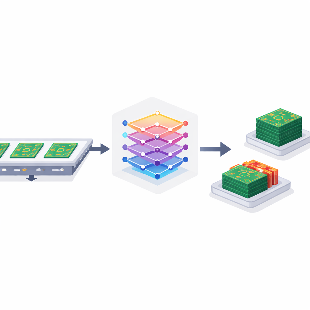
Every modern gadget—from smartphones to medical devices—depends on printed circuit boards (PCBs), the green plates that route electrical signals. As electronics shrink and become more complex, these boards can hide hairline breaks, microscopic holes, and specks of stray metal that are nearly impossible for humans to spot. The paper introduces a new artificial intelligence system, called PCB‑YOLOv8X, designed to automatically find these tiny defects quickly and accurately, helping manufacturers catch problems before faulty products reach consumers.
The challenge of seeing the nearly invisible
Today’s PCBs pack dense forests of copper lines, shiny solder pads, and printed markings into very small areas. That busy background, combined with reflections and noise in camera images, makes small flaws easy to miss. Traditional machine vision systems rely on fixed rules and simple comparisons between a “good” reference image and a test board. They can work for large or obvious defects, but often fail when defects are irregularly shaped, extremely small, or appear under changing lighting conditions. Deep learning has improved matters by learning patterns directly from data, yet many existing models still struggle with irregular shapes and distant context, leading to missed defects and false alarms.
A smarter way to scan circuit boards
PCB‑YOLOv8X builds on a popular real‑time object detection framework and tailors it specifically for PCB inspection. The network is organized into three stages: a “backbone” that extracts visual features from images, a “neck” that fuses information across different scales, and a “head” that decides where defects are and which type they are. The authors redesign key parts of this pipeline so the model can better follow the fine, twisting paths of copper traces and distinguish meaningful flaws from harmless background textures. The overall goal is to capture more detail about tiny defects while keeping the system fast enough for in‑line industrial use.
Flexible vision and focused attention
The first major upgrade lets the model adapt its “gaze” to irregular shapes. Instead of sampling image information on a rigid grid, the new C2f‑DCNV2 module uses deformable filters whose sampling points can shift slightly to follow bent traces, jagged edges, or irregular gaps. This flexibility helps the network latch onto the true outlines of small defects such as missing holes, mouse‑bite patterns, or short circuits. The second upgrade, the SPPF‑LSKA module, gives the model a wider field of view while remaining efficient. It mimics looking both close‑up and from afar by combining information from multiple scales, then uses an attention mechanism to emphasize regions that are likely to contain defects and downplay distracting background patterns.
Sharper decisions about tiny targets
Finding a defect is only half the battle; the system must also draw a tight box around it. Standard training methods judge these boxes based mainly on how much they overlap with the true defect area, which can fail when defects are very small or do not overlap at all. The authors introduce a refined training objective, called IWD‑CIoU, which measures how close and similar predicted and true boxes are using a distance concept borrowed from probability theory. This approach provides useful feedback even when two boxes barely touch and helps the network learn to localize minuscule flaws more precisely. It also pairs this distance measure with a classification strategy that stresses high‑confidence examples and hard‑to‑distinguish cases.
From lab tests to factory lines
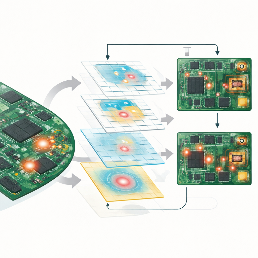
The team evaluates PCB‑YOLOv8X on a public PCB defect dataset containing six common flaw types, from open circuits to spurious copper. After augmenting the data to mimic real production variability, they compare their model with widely used detectors such as Faster R‑CNN, SSD, several generations of YOLO, and a transformer‑based method. PCB‑YOLOv8X achieves the highest overall accuracy, correctly identifying and localizing defects in more than 98% of cases while also running faster than the baseline YOLOv8 model. Visual heatmaps show that the improved network concentrates strongly on actual defect regions and largely ignores confusing textures and reflections, reducing both missed defects and false positives. The authors note remaining challenges—such as extremely tiny, low‑contrast flaws and confusing background patterns—and propose future work using lighter models and synthetic training data to better support edge devices on production lines.
What this means for everyday electronics
In practical terms, PCB‑YOLOv8X could sit behind high‑speed cameras on a factory line, scanning each passing board in real time and flagging suspect pieces for human review. By spotting microscopic defects that older systems overlook, it can help manufacturers prevent hidden faults that might later cause device failures or safety issues. For non‑specialists, the take‑home message is that advances in tailored AI vision are making the invisible visible on the factory floor, quietly improving the reliability of the electronics we rely on every day.
Citation: Xu, X., Dela Cruz, J.C. & Wang, Y. PCB-YOLOV8X: a network for detecting micro-sized defects on PCB surfaces based on enhanced feature information. Sci Rep 16, 10860 (2026). https://doi.org/10.1038/s41598-026-46089-6
Keywords: PCB defect detection, computer vision, deep learning, quality control, manufacturing automation