Clear Sky Science · en
Super-resolution approach tailored for wafer transmission electron microscopy images
Sharper Views Inside Computer Chips
Modern electronics depend on tiny structures etched deep inside semiconductor wafers, but clearly imaging these features is slow, expensive, and technically demanding. This study shows how advanced image-processing techniques can turn blurry, noisy microscope pictures of wafers into crisp, high‑resolution views, without having to recapture them on costly equipment. The result is a practical recipe that could speed up defect detection and measurements in chip factories, while cutting the time experts spend at specialized microscopes.
Why Seeing Below the Surface Matters
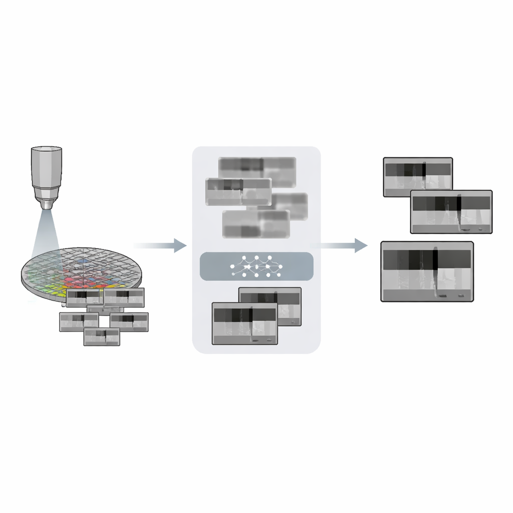
Chip makers already use several kinds of images to keep production on track. Surface-level pictures, such as wafer maps and scanning electron microscope images, can reveal many kinds of flaws, but they miss what happens inside the material. Transmission electron microscopy (TEM) goes deeper by shooting electrons through thin slices of the wafer to reveal atomic-scale structure, hidden defects, and material composition. These high-resolution TEM images are extremely valuable, yet they are hard to obtain in large numbers because preparing and imaging each sample destroys the wafer and requires expert operators and long imaging sessions.
The Trouble with Blurry and Noisy Images
In principle, a clever computer program could transform low-resolution wafer TEM images into high-resolution ones, a task known as super-resolution. In practice, wafer TEM images pose special challenges. First, the noise patterns are unusual, caused by scattered electrons and unstable magnetic fields rather than ordinary camera noise, so off‑the‑shelf cleaning methods work poorly. Second, small features along boundaries and edges are exactly where engineers look for defects or measure layer thickness, yet these edges tend to blur when resolution is low. Finally, the usual way to train super-resolution models—using perfectly matched pairs of blurry and sharp images of the same scene—is not feasible here, because chip makers typically only store the high‑resolution TEM images.
A Three-Step Recipe for Better Images
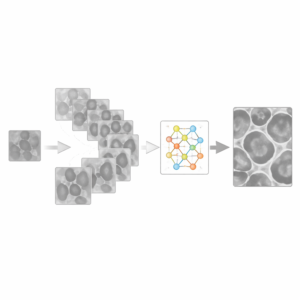
To overcome these obstacles, the authors design a three-stage framework tailored to wafer TEM data. In the first stage, called practical degradation, they start from high‑resolution images and deliberately generate many different low‑quality versions by shuffling the order and strength of blur, downsampling, noise, and compression. A particularly rich version of this process, named Hybrid, creates a broad range of realistic distortions that mimic the unknown noise patterns seen in real factories. In the second stage, image enhancement, they take the original high‑resolution images and push the edges to become even crisper using a method called HighboostFiltering, which strongly highlights boundaries without adding extra trainable complexity. These synthetic low‑ and “extra‑sharp” high‑resolution pairs then form the training data for the third stage, where a super-resolution model learns to turn poor images into clear ones.
Finding the Best Combination
The team systematically tests 48 combinations of degradation strategies, enhancement methods, and model types. They compare a traditional convolutional network, a generative adversarial network (ESRGAN), and a diffusion-based model (SR3). Image quality is judged using a metric that estimates how natural an image looks without needing a ground-truth reference. The clear winner is a previously unexplored trio: Hybrid degradation, HighboostFiltering enhancement, and the ESRGAN model. This combination produces images that most closely resemble those captured manually by TEM experts, with smoother noise and much sharper edges. In contrast, diffusion-based models struggle with the small, specialized dataset and often produce unstable or noisy results.
From Prettier Pictures to Better Decisions
Improved images are only useful if they help with real factory tasks. To test this, the authors feed the super-resolved images into a powerful general-purpose segmentation tool to perform defect-like region detection and edge extraction, without retraining that tool. Compared with both raw low-resolution inputs and nine existing super-resolution methods, the proposed combination delivers noticeably better segmentation scores and crisper edges, both of which are crucial for measuring fine structures and spotting subtle flaws. Although some failure cases remain—such as occasional noisy patches or artifacts from unmodeled noise—the study demonstrates that a carefully designed three-step pipeline can make low-resolution wafer TEM images far more informative. For a non-specialist, the key takeaway is that by cleverly fabricating training data and emphasizing edges, the authors turn existing blurry microscope images into sharper diagnostic tools, helping the semiconductor industry see more while imaging less.
Citation: Kim, S., Baek, I., Cho, H. et al. Super-resolution approach tailored for wafer transmission electron microscopy images. Sci Rep 16, 10662 (2026). https://doi.org/10.1038/s41598-026-45776-8
Keywords: super-resolution, transmission electron microscopy, semiconductor manufacturing, image enhancement, deep learning