Clear Sky Science · en
A SMT pin soldering defect detection system based on improved connectivity domain algorithm
Why tiny solder joints matter
Modern electronics, from phones to cars, are built on circuit boards packed with tiny metal pins and shiny solder joints. If even a few of these joints accidentally melt together, they can short a circuit, damage parts, or cause mysterious failures in finished products. This study shows how a smarter camera-based inspection method can spot those hidden mistakes more reliably, helping factories keep quality high without slowing production.
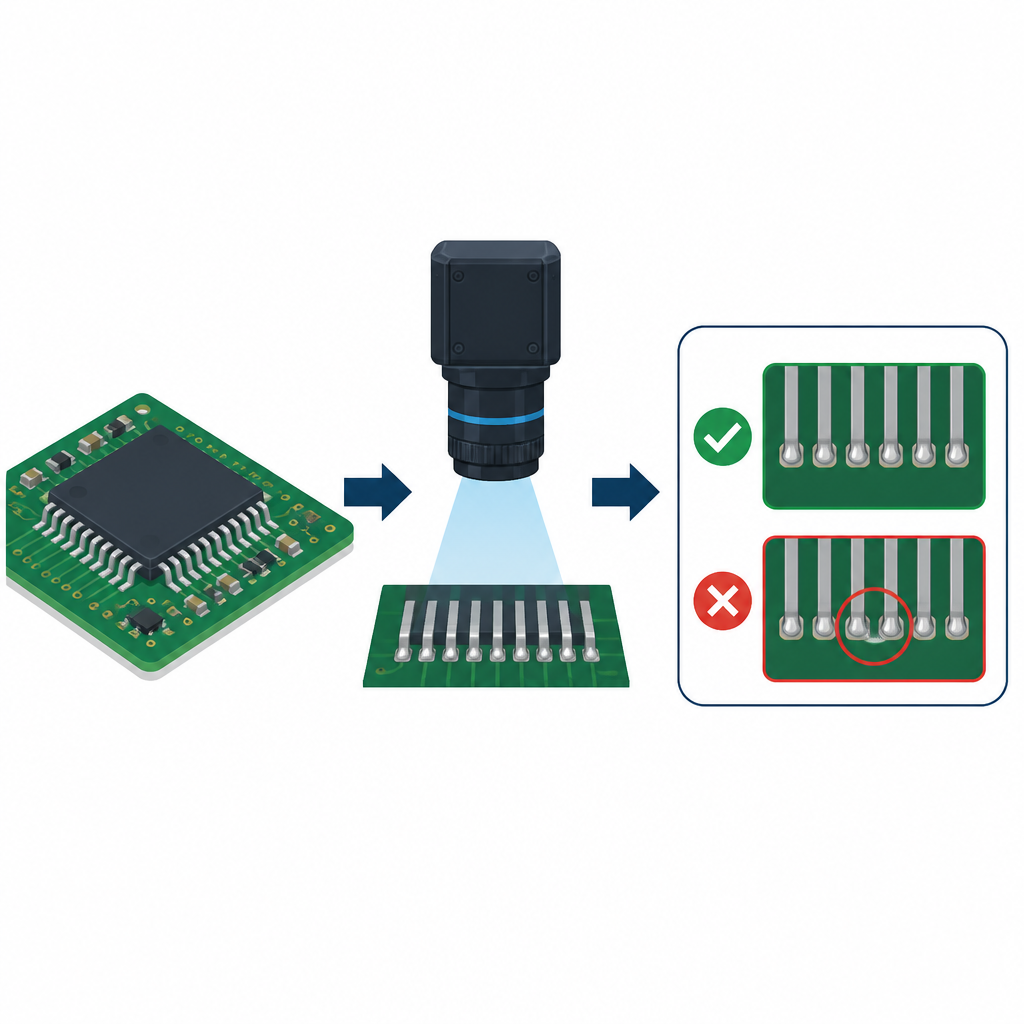
Looking for trouble with digital eyes
To check solder joints automatically, factories often rely on machine vision systems: cameras take close-up pictures of boards, and software scans each pixel to decide which areas belong to metal pins, which to solder, and which to the background. A popular approach treats each continuous patch of bright pixels as a separate region and counts how many pixels it contains. A normal solder joint has a typical size range, while a bridge that connects two pins tends to be much larger. In simple layouts with plenty of space between pins, this counting method works well, quickly flagging overly large regions as likely defects.
When parts are packed too tightly
As manufacturers shrink devices and crowd more parts onto each board, gaps between pins become extremely small. In these dense areas, standard region-counting can be fooled: two neighboring pins that are correctly soldered may appear to merge into one region in the image, causing the software to mislabel them as a bridge. Noise in the picture and weak edges around the solder can make this problem worse, leading to false alarms that slow down inspection and may even hide real faults behind a flood of mistaken warnings.
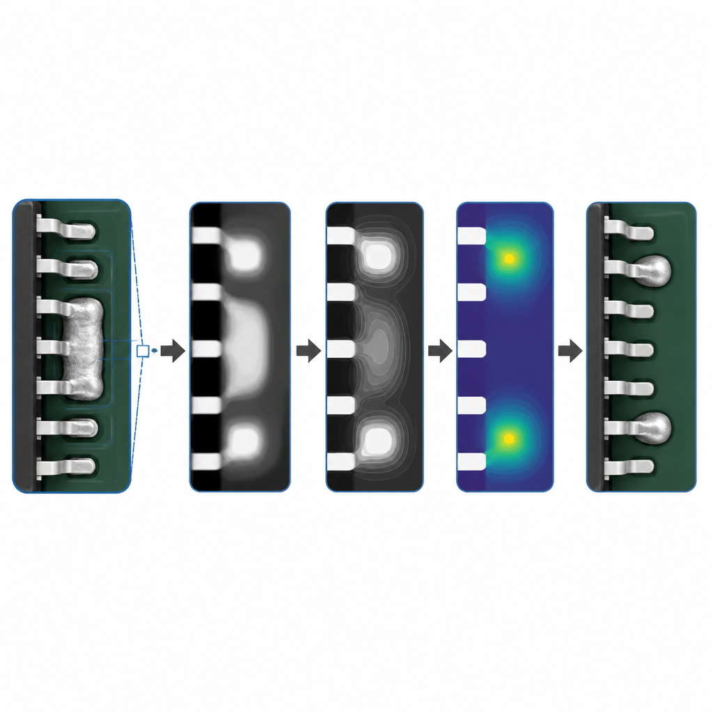
A two-step way to separate what seems stuck together
The researchers tackle this issue by keeping the speed of the traditional method but adding a focused second look wherever the first step might have gone wrong. The system first runs the usual region-labeling and pixel-counting to find suspect areas that appear too big. Instead of accepting those as defects outright, it cuts them out as small patches and enhances the contrast inside them so subtle boundaries become clearer. Next, it uses a distance-based trick that measures how far each point is from the edge of the region, creating a smooth landscape where the centers of solder blobs look like hills and the spaces between them look like valleys.
Letting virtual water find hidden borders
On this artificial landscape, the team applies a process called a watershed, which imagines water filling up the valleys and meeting at invisible ridge lines. These ridges mark likely borders between separate solder joints that looked fused at first glance. By applying this only inside the suspect patches, the method keeps computing demands low while carefully splitting apart pins that were mistakenly merged. The newly separated regions are then dropped back into the original image, and the region-counting step is run again, this time on a cleaner, more accurate picture of the joints.
Proof from real circuit boards
To test the system, the authors built a practical inspection setup with an industrial camera and a LabVIEW-based program, and applied it to a mix of public test images and boards from their own lab. They measured how often the system correctly caught real solder bridges and how often it cried wolf. Across 300 test images, the improved method kept high accuracy while sharply reducing false positives on tightly packed pins. It was able to distinguish true solder bridges from harmless close neighbors and remained stable under different layouts and lighting conditions.
What this means for everyday electronics
For non-specialists, the takeaway is that this approach gives circuit-board makers a more dependable pair of digital eyes. By combining a fast first pass with a targeted second analysis, the system can better separate truly dangerous solder bridges from harmless joints that only look suspicious. This makes inspection more trustworthy and less sensitive to cluttered layouts, helping to ensure that the tiny metal connections inside everyday devices work as intended throughout their lives.
Citation: Xiong, W., Xiao, N. & Wang, R. A SMT pin soldering defect detection system based on improved connectivity domain algorithm. Sci Rep 16, 14789 (2026). https://doi.org/10.1038/s41598-026-44847-0
Keywords: solder bridge detection, machine vision, SMT inspection, image segmentation, circuit board quality