Clear Sky Science · en
Sol–gel synthesis and comprehensive characterization of MgO nanostructures: structural, optical, and dielectric insights
Why Tiny Grains of a Common Mineral Matter
Magnesium oxide is a simple, inexpensive ceramic used in everything from furnace linings to pharmaceuticals. This study shows that when MgO is made from the bottom up as nanoparticles, its internal imperfections can be deliberately shaped to give it new optical and electrical behaviors. That means an everyday material could be redesigned for modern needs such as UV‑blocking coatings, microelectronic insulators, and even environmental cleanup, simply by controlling how it is synthesized.

Building Nanoparticles Drop by Drop
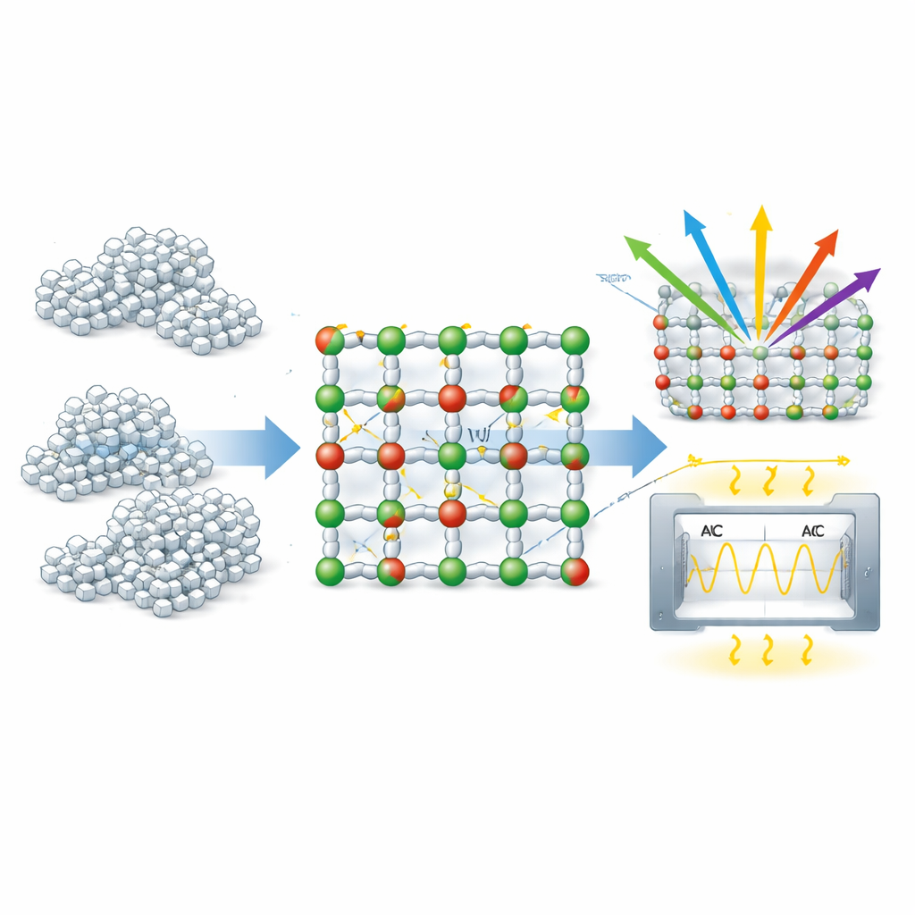
The researchers created magnesium oxide nanostructures using a wet‑chemistry approach called the sol–gel method. In this process, a clear solution of magnesium salts and citric acid is slowly converted into a gel and then heated to form a fine white powder. This route gives excellent control over chemical uniformity but also tends to introduce many tiny structural flaws. X‑ray diffraction measurements showed that the final material is a well‑crystallized cubic phase of MgO, with building blocks only about 30–50 nanometers across. Detailed mathematical analysis of the diffraction peaks revealed that these tiny crystals are under strain and contain stacking faults—places where the regular sequence of atomic layers has been disturbed.
Tuning the Inside of the Crystal
By refining the X‑ray data, the team could map how magnesium and oxygen atoms are arranged and even estimate how many sites are left vacant. In an ideal MgO crystal, every magnesium site and every oxygen site would be filled. Here, both types of sites were slightly under‑occupied, evidence of so‑called Schottky defects—paired vacancies of magnesium and oxygen. Electron density maps confirmed a face‑centered cubic framework but with these built‑in absences and distortions. Comparing several advanced models for peak broadening, the authors concluded that the most reliable description is a lattice made of ~30 nm coherently ordered regions, separated by defect‑rich boundaries that carry significant strain. High‑resolution electron microscopy backed this up: particles seen in the microscope were often larger agglomerates made of several such strained crystallites clumped together.
How Defects Change the Way Light and Electricity Flow
These subtle structural changes have dramatic consequences for how the material interacts with light. Using ultraviolet–visible spectroscopy, the researchers found that the nanoparticles start absorbing strongly around 276 nanometers, corresponding to an effective optical band gap of about 4.48 electron volts—far smaller than the ~7.8 eV gap of bulk MgO. Instead of being a nearly perfect insulator to ultraviolet light, the nanostructured material can absorb a broader range of UV photons. An analysis of the so‑called Urbach tail, a gentle slope in the absorption edge, yielded an Urbach energy of about 168 millielectron volts, a clear signature of many defect‑related electronic states spilling into the band gap. In simple terms, the vacancies and distortions create extra “stepping stones” that allow electrons to move with less energy than in a flawless crystal.
Electric Response Shaped by Grains and Gaps
The team also measured how the nanoparticles respond to alternating electrical fields across a wide range of frequencies. The electrical conductivity increased steadily with frequency in a way that matches a well‑known empirical rule for disordered solids, indicating that charge carriers hop between localized defect sites rather than flowing freely. Impedance measurements plotted in a Cole–Cole diagram showed a single broad semicircle, meaning that the dominant response comes from the interiors of the grains, not from the boundaries between them. The dielectric constant and energy loss both decreased as frequency rose, reflecting the fact that slow polarization mechanisms—such as charges piling up at interfaces—cannot keep up with rapidly changing fields. At high frequencies, only the fastest, low‑loss polarization of ions and electrons remains, pointing to good performance as a high‑frequency insulating layer.
What This Means for Future Devices
Taken together, the results establish a direct link between how these MgO nanoparticles are made, the defects and strain locked into their crystal lattice, and the way they handle light and electricity. By tailoring the sol–gel processing conditions, it should be possible to “engineer” the concentration of vacancies and the level of internal strain, and thus dial in a desired band gap and dielectric behavior. That makes this common ceramic a tunable platform for UV filters, transparent protective coatings, high‑quality insulating films in microelectronics, gas sensors, and photocatalysts for breaking down pollutants—all achieved not by changing the chemistry, but by reshaping the material from the nanoscale inward.
Citation: AbdelAll, N., Mimouni, A., Rayan, A.M. et al. Sol–gel synthesis and comprehensive characterization of MgO nanostructures: structural, optical, and dielectric insights. Sci Rep 16, 12215 (2026). https://doi.org/10.1038/s41598-026-44397-5
Keywords: magnesium oxide nanoparticles, sol–gel synthesis, defect engineering, optical band gap, dielectric properties