Clear Sky Science · en
Adaptive reinforcement learning for lithography optimization: a scalable AI-driven solution for next-generation semiconductor manufacturing
Smaller Chips, Bigger Challenges
Every year, our phones, laptops, and data centers rely on computer chips with features carved just a few billionths of a meter wide. At these scales, simply shining light through a patterned "stencil" to draw circuits on silicon stops behaving in an easy, predictable way. The patterns blur, distort, and change with tiny shifts in focus or light intensity, threatening yield and driving up cost. This paper presents a new artificial-intelligence–driven method, called Adaptive Reinforcement Learning for Lithography Optimization (ARLO), designed to keep chip manufacturing accurate, fast, and affordable as industry pushes below the 5‑nanometer frontier. 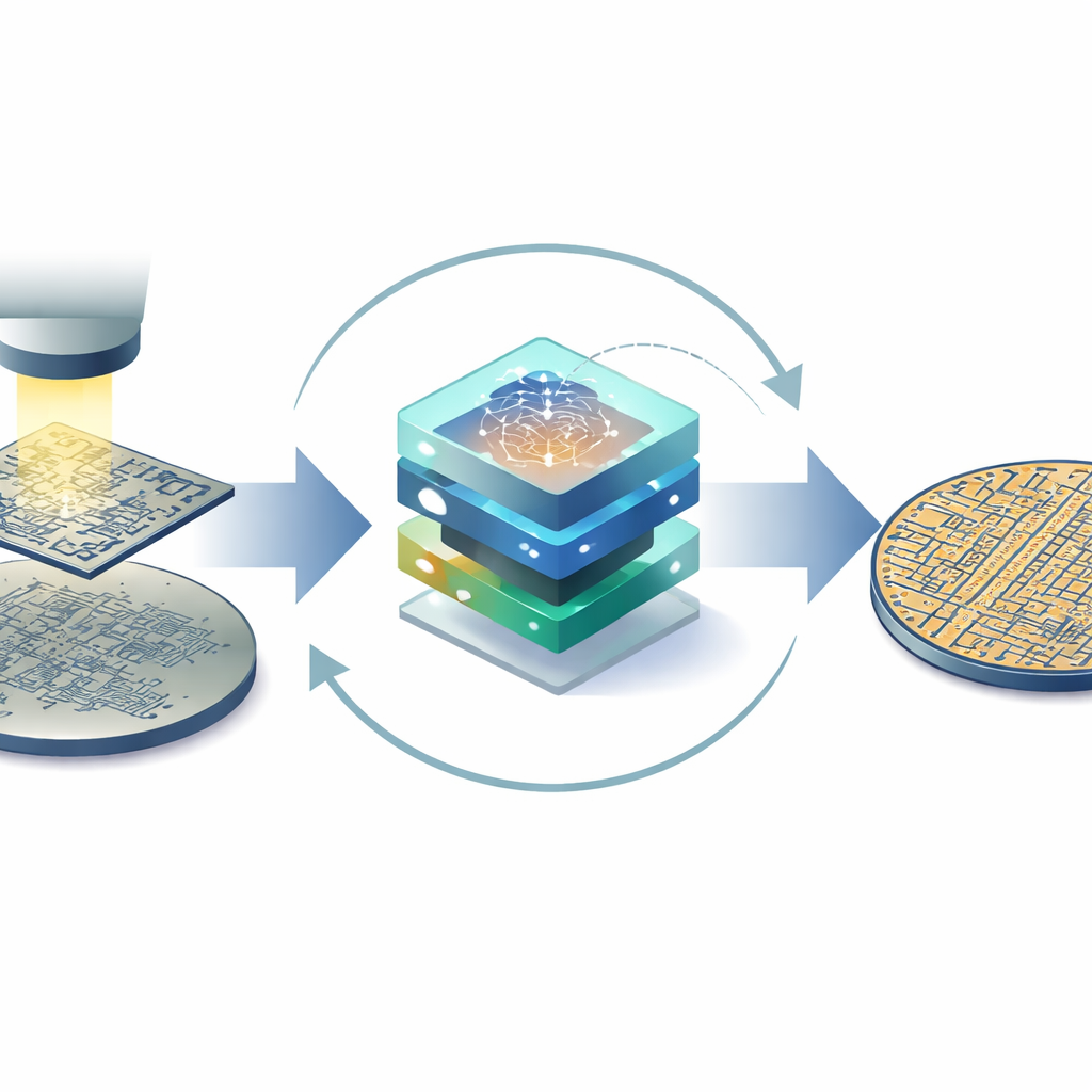
How Chips Are Printed Today
Modern chips are made using lithography, a process that projects light through a patterned mask onto a light-sensitive coating on a silicon wafer. Ideally, the image on the wafer matches the intended circuit drawing. In reality, light diffracts, nearby shapes interact, and the chemicals in the coating respond in complex ways. To compensate, engineers pre-distort the mask so that, after all these effects, the wafer pattern comes out right. Traditional methods, such as Optical Proximity Correction and more advanced Inverse Lithography Technology, treat this as a carefully tuned math problem: given a desired pattern, compute the mask that will produce it. These approaches can be very precise but grow painfully slow and computationally expensive for full chips, and they often produce masks packed with tiny fragments that are costly to manufacture.
Why Conventional Methods Are Hitting a Wall
As features shrink below the wavelength of the light used in extreme ultraviolet lithography, small errors become huge headaches. Standard techniques require many iterative calculations for each small tile of the layout, and when repeated across hundreds of thousands of tiles, turn into a major bottleneck. They can also generate extremely intricate mask shapes, which increase the number of tiny "shots" an electron-beam tool must write when making the mask, boosting time and cost. At the same time, factories need masks that still work even if focus or exposure drift slightly away from their ideal settings. Balancing accuracy, robustness, and manufacturability with older tools is increasingly difficult, and this is where the authors argue that a new AI-centered strategy is needed.
An AI Coach for Better Lithography Masks
ARLO tackles the problem by combining two powerful ideas from machine learning. First, a U‑Net–style image-processing network provides a fast starting guess for the mask, given the desired circuit pattern. This network is trained on many examples so that it learns typical corrections and global layout context, such as dense wiring regions and sharp corners. Second, a reinforcement learning agent acts like a coach that repeatedly tweaks this initial mask and tests it in a realistic lithography simulator. After each round, the agent receives a single score that blends several goals: how closely the printed pattern matches the target, how stable it remains under focus and dose variations, how well edges line up, and how complex the mask is to manufacture. By rewarding good trade-offs and penalizing poor ones, the agent learns a strategy for refining masks in a small number of steps. 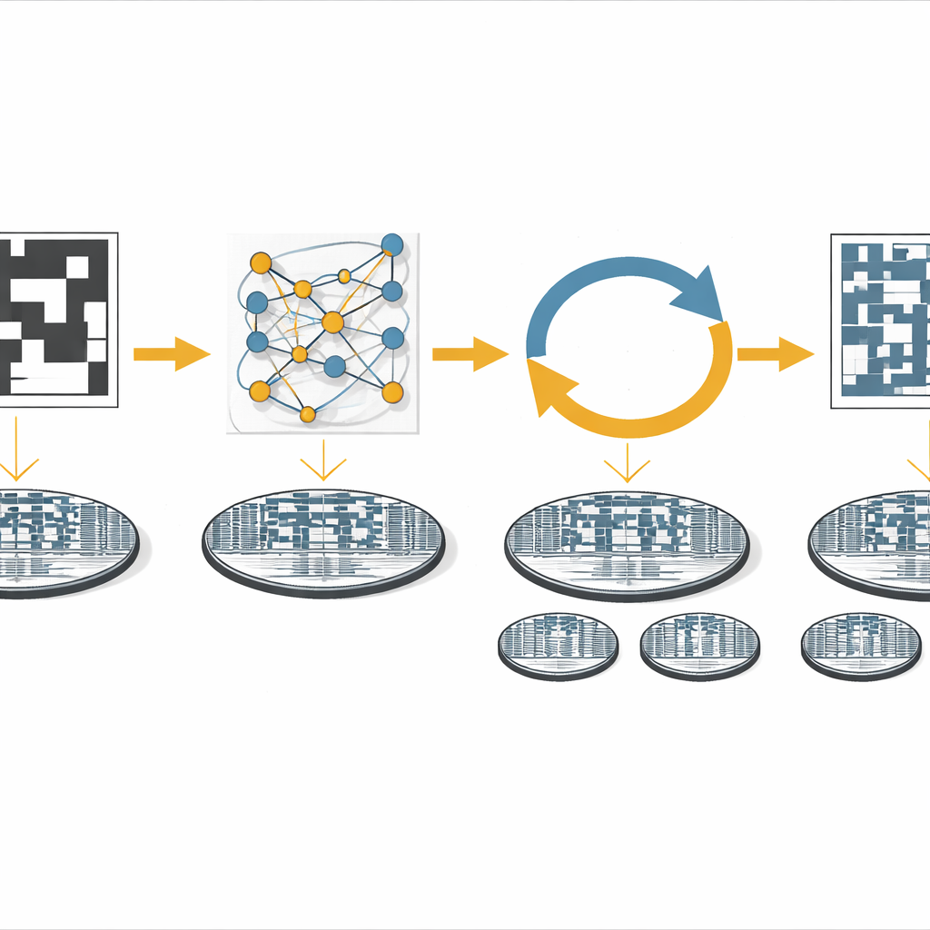
Testing on Realistic Chip Patterns
To prove that ARLO is more than a lab curiosity, the authors benchmarked it on LithoBench, a large open dataset that mimics realistic chip designs across different layers: dense metal wiring, vertical connections between layers, and standard logic patterns. Under extreme ultraviolet conditions, ARLO is compared head‑to‑head with several leading methods, including systems based on generative adversarial networks, purely deep-learning U‑Net models, and earlier reinforcement-learning–based lithography tools. Across tens of thousands of layout tiles, ARLO consistently reduces the mismatch between desired and printed images and shrinks the range of variation caused by process changes. Importantly, these gains come with a per‑tile runtime of only a few hundredths of a second on a modern graphics processor, suggesting that full-chip application within practical time limits is realistic.
Trade-Offs and What This Means for Future Chips
ARLO does not optimize everything at once: its masks tend to be more detailed, increasing the number of features that must be written on the mask plate. However, this added complexity pays off in significantly sharper and more reliable wafer patterns. The method cuts error in the printed intensity by more than a third and slashes sensitivity to process variation by well over half when compared with prominent existing approaches, all while keeping computation within factory-friendly limits. To a non-specialist, the bottom line is that ARLO shows how a smart, feedback-driven AI can work alongside physics-based simulators to push lithography further, helping the semiconductor industry continue shrinking transistors without an explosion in cost or design time.
Citation: Rashid, U., Shafique, F., Atif, H. et al. Adaptive reinforcement learning for lithography optimization: a scalable AI-driven solution for next-generation semiconductor manufacturing. Sci Rep 16, 13589 (2026). https://doi.org/10.1038/s41598-026-43555-z
Keywords: computational lithography, semiconductor manufacturing, reinforcement learning, photomask optimization, extreme ultraviolet lithography