Clear Sky Science · en
Effect of temperature on 2D terahertz plasmons in AlGaN/GaN heterostructures
Why tiny ripples of charge matter
Wireless links, airport scanners, and next‑generation chips increasingly rely on terahertz waves—radiation that sits between microwaves and infrared light. One promising way to generate and detect these waves is to use plasmons, tiny ripples of electrical charge, in advanced semiconductor structures. This study asks a deceptively simple question with big engineering consequences: how does temperature change the behavior of these ripples in gallium nitride–based devices, from chilly laboratory conditions up to room temperature?
Ripples of charge on a flat highway
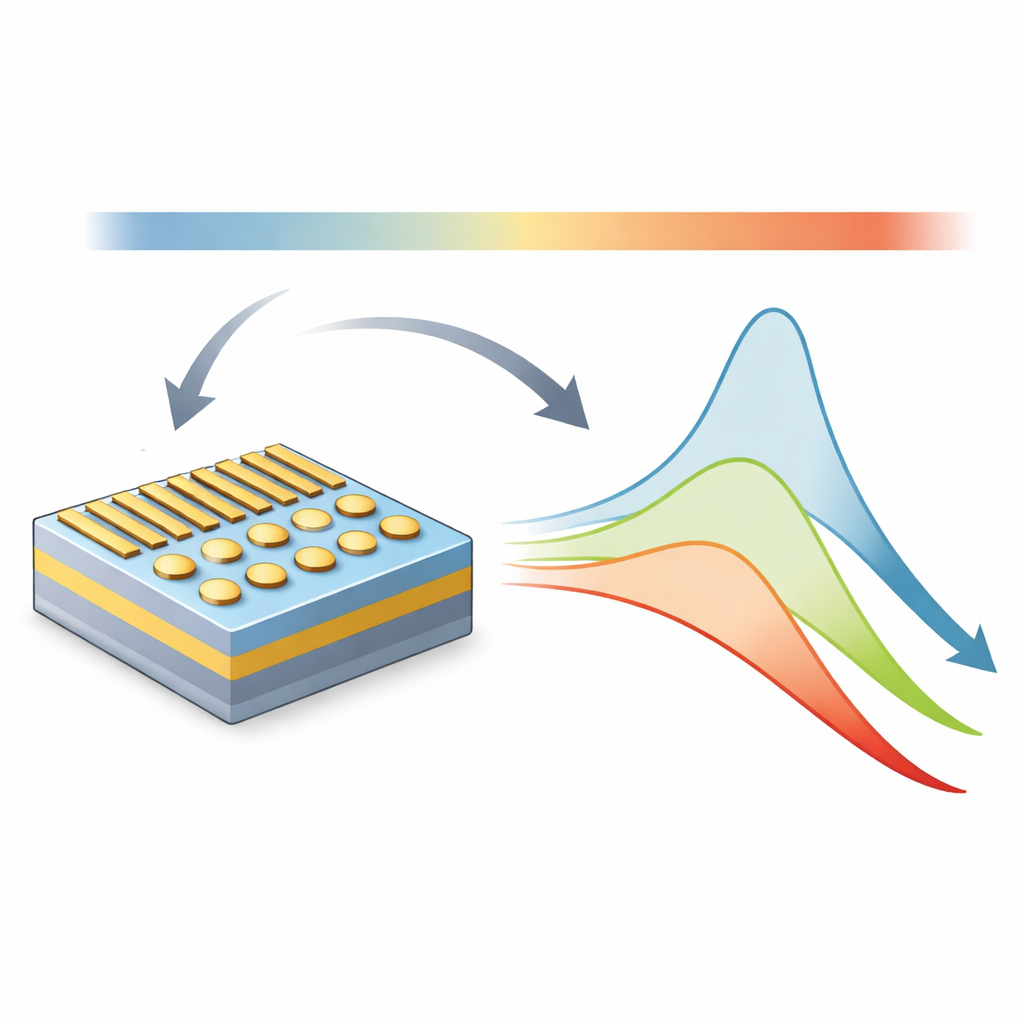
In the devices examined here, electrons are confined to move in an ultra‑thin sheet, forming what physicists call a two‑dimensional electron gas. When these electrons slosh back and forth collectively, they create plasmons whose natural rhythm falls in the terahertz range if the sheet is dense enough and patterned on micrometer scales. The team builds “plasmonic crystals” by either placing a metal grating on top of the semiconductor or by etching it into a regular array of tiny disks. These repeating structures act like a man‑made crystal for charge waves, shaping how terahertz radiation is absorbed and transmitted.
Two kinds of waves in one device
Depending on the applied voltage, the charge oscillations can spread across both the covered and uncovered regions (a delocalized mode) or be confined mainly to the uncovered regions (a localized mode). The localized waves tend to vibrate at higher frequencies because the electrons in the exposed regions feel less screening from metal above them. By shining broad‑band terahertz light through large arrays of these structures at different temperatures, and tracking how specific absorption peaks move, the researchers map how both types of modes shift as the sample is warmed and cooled.
Temperature, trap states, and a moving target
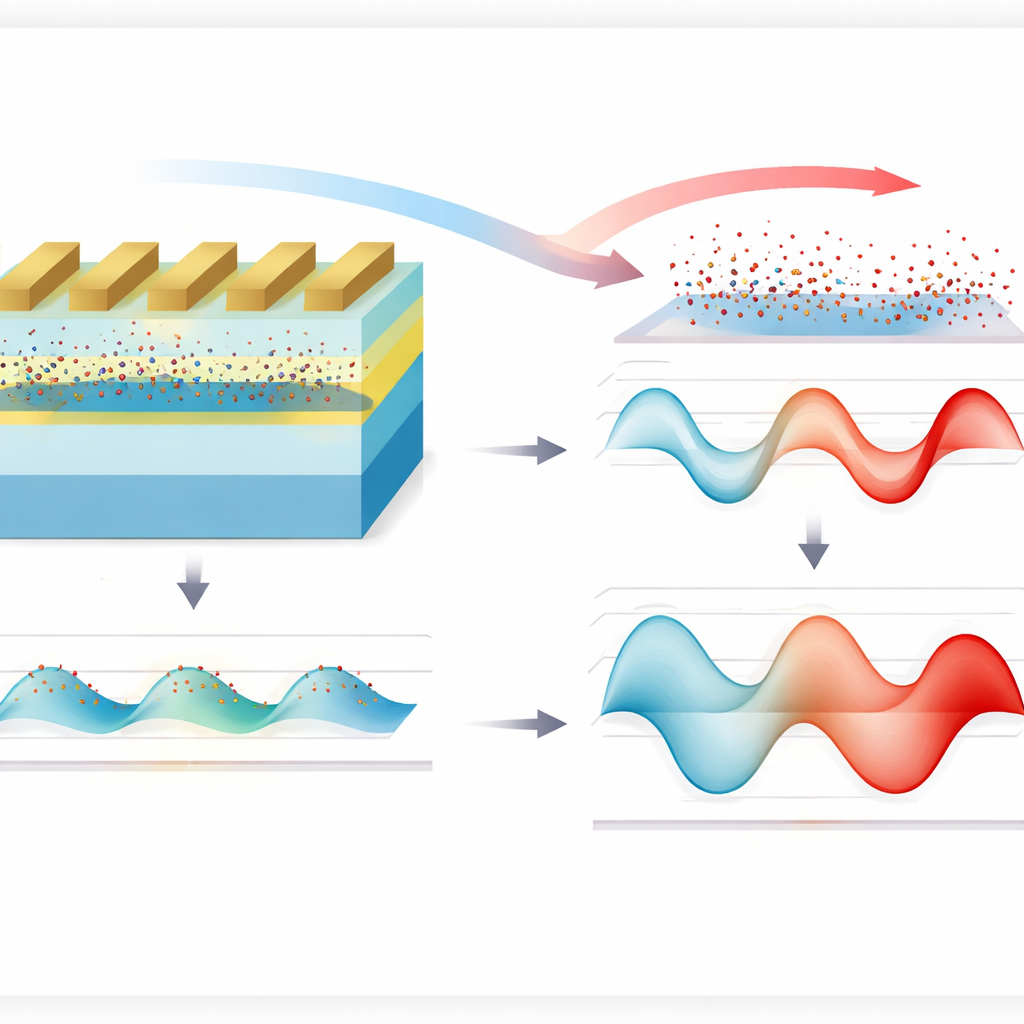
As temperature rises, the resonance frequency of both localized and delocalized plasmons generally drifts downward—a redshift. But the shift is not smooth or identical from device to device. Instead, it shows hysteresis (the warming and cooling curves do not match) and large sample‑to‑sample variation. The authors rule out two obvious explanations: the electron density under the metal gates remains essentially constant with temperature, as confirmed by transistor measurements, and the material’s dielectric constant changes only weakly. The culprit turns out to be the exposed semiconductor surface between metal features. Imperfections and “surface states” there can trap and release charge slowly as temperature, light, and ambient conditions change, subtly altering the electron density in the uncovered regions and effectively changing the length and strength of the plasmon cavities.
Weighing electrons as the chip warms up
Another suspect is the electrons’ effective mass—the inertia electrons appear to have inside the crystal. Because the plasmon frequency depends on this mass, any change with temperature could shift the resonances. However, the complicated and sample‑specific surface effects make it hard to deduce the mass just from plasmon measurements. To bypass the surface altogether, the team performs cyclotron resonance experiments on a plain wafer, using a magnetic field and single‑frequency terahertz light to track how electrons orbit in the material. From the shifting absorption lines, they find that the effective mass of electrons in gallium nitride grows significantly—by roughly a factor of 1.5 to 2—between about 70 and 290 kelvin. This growth, together with the changing surface charge, jointly explains the observed redshift of plasmon resonances.
What this means for future terahertz chips
For designers of high‑power transistors, light sources, and terahertz detectors based on gallium nitride, these findings carry a clear message: the basic “weight” of electrons and the behavior of exposed surfaces cannot be treated as fixed background details. As devices heat during normal operation, both the effective mass and the surface‑controlled electron density in uncovered regions change enough to noticeably move plasmon resonances. Ignoring these effects could lead to terahertz components that drift off‑frequency or behave inconsistently from chip to chip. Accounting for surface states and temperature‑dependent effective mass in design and modeling should make GaN‑based terahertz electronics more reliable, tunable, and ready for real‑world environments.
Citation: Dub, M., Sai, P., Yavorskiy, D. et al. Effect of temperature on 2D terahertz plasmons in AlGaN/GaN heterostructures. Sci Rep 16, 12163 (2026). https://doi.org/10.1038/s41598-026-41524-0
Keywords: terahertz plasmons, gallium nitride, plasmonic crystals, effective mass, surface states