Clear Sky Science · en
Investigating the optoelectronic properties and photovoltaic performance of Na2AuGaBr6 based double perovskite solar cells via numerical simulation and AI techniques
Cleaner Power from a New Kind of Crystal
Solar panels are getting better every year, but many of the most efficient designs still rely on lead, a toxic metal. This study explores a promising lead‑free alternative built from a specialty crystal called Na2AuGaBr6 and shows, using computer models and artificial intelligence, that it could reach efficiencies rivaling or surpassing today’s commercial solar cells—without the environmental drawbacks.
A Safer Path Beyond Silicon and Lead
Traditional silicon panels are reliable but costly to manufacture, and next‑generation “perovskite” solar cells, while highly efficient, often contain lead. The material examined here, Na2AuGaBr6, belongs to a family known as double perovskites that replace lead with less hazardous elements such as sodium, gold and gallium bound to bromine. The researchers first used quantum‑level calculations to check whether this crystal is structurally stable and how it interacts with light. They found that it forms a robust cubic lattice and behaves as a direct band‑gap semiconductor with an energy scale well‑matched to sunlight—meaning it should absorb light efficiently and convert it into mobile electrical charges.
Designing the Ideal Solar Stack
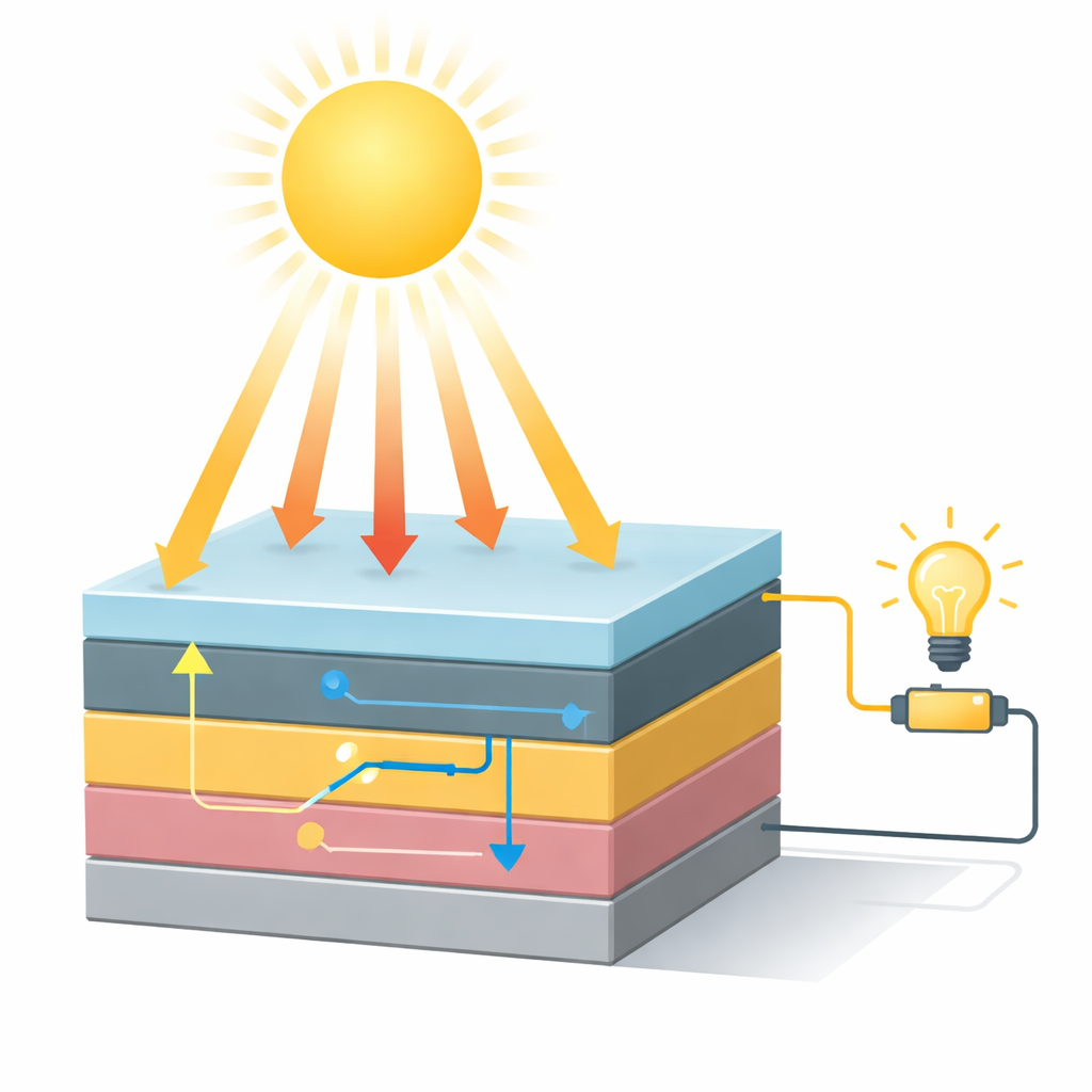
A solar cell is more than just a light‑absorbing layer. It also needs supporting layers that guide electrons and positive charges to opposite sides without letting them leak or recombine. Using a specialized simulation tool, the team virtually built 48 different device layouts around Na2AuGaBr6, swapping in various materials above and below the absorber. They discovered that a particular combination—an aluminum front contact, a transparent oxide, a layer of tungsten disulfide to carry electrons, the Na2AuGaBr6 absorber, a thin layer of vanadium oxide to carry positive charges and a nickel back contact—performed best. In this configuration, the simulated device reached a power conversion efficiency of about 29 percent, higher than most panels on rooftops today.
Fine‑Tuning Thickness, Defects and Contacts
The study then asked a practical question: how sensitive is performance to real‑world imperfections? By varying layer thicknesses, electrical doping (how many extra charges a material can provide), and the density of defects in the bulk crystal and at interfaces, the authors mapped out where the design is most vulnerable. They found that making the absorber about one micrometer thick offered a sweet spot between strong light absorption and minimal charge loss. Too many defects, either inside the absorber or at the boundaries between layers, quickly reduced voltage and current. Careful choice of contact metals also mattered: aluminum and nickel, with their complementary abilities to collect electrons and positive charges, gave the best match to the internal energy levels and minimized wasted energy.
Letting Artificial Intelligence Steer the Search
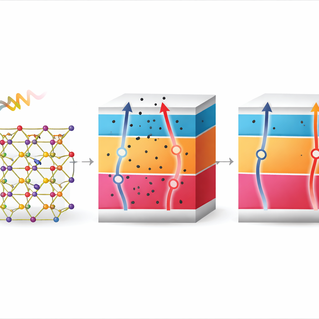
Exploring every possible combination of thickness, defects and materials experimentally would be slow and expensive. To speed things up, the researchers trained several machine‑learning and deep‑learning models on data from their numerical solar‑cell simulations. These algorithms learned to predict key performance numbers—such as efficiency and output current—from the input design parameters. Among eleven tested approaches, a method called Gradient Boosting delivered the most accurate forecasts, closely matching the detailed physics simulations. It also highlighted which factors matter most: defect density, how strongly the absorber is doped and operating temperature emerged as the primary levers for boosting efficiency.
The Big Picture for Future Solar Panels
In plain terms, this work shows that a carefully engineered, lead‑free Na2AuGaBr6 crystal, paired with the right supporting layers, could underpin solar cells approaching 30 percent efficiency—comparable to the best lab devices but with a cleaner chemical makeup. Just as important, the combination of quantum calculations, device‑level simulations and AI‑based prediction offers a powerful blueprint for discovering and optimizing new solar materials. If confirmed in the lab, designs like this could help deliver cheaper, greener and more efficient solar panels, accelerating the shift away from fossil fuels while reducing concerns about toxic ingredients.
Citation: Biswas, B.C., Shimul, A.I., Paul, I. et al. Investigating the optoelectronic properties and photovoltaic performance of Na2AuGaBr6 based double perovskite solar cells via numerical simulation and AI techniques. Sci Rep 16, 11218 (2026). https://doi.org/10.1038/s41598-026-41519-x
Keywords: lead-free perovskite solar cells, double perovskite Na2AuGaBr6, photovoltaic device simulation, machine learning for solar materials, high-efficiency thin-film photovoltaics