Clear Sky Science · en
Insilico investigations of the physical properties of hexagonal chalcogenide perovskites CsXS3 (X = Nb, V) for UV optoelectronic devices and photovoltaic applications
New Materials for Future Solar Power
As the world moves toward cleaner energy, scientists are searching for durable, non-toxic materials that can turn sunlight into electricity more efficiently. This study explores two little-known compounds, CsNbS3 and CsVS3, that belong to a family called chalcogenide perovskites. Using advanced computer simulations instead of lab experiments, the authors examine how these crystals are built, how they conduct electricity, and how well they absorb light. Their goal is to see whether these materials could serve in next-generation solar cells and ultraviolet detectors, and to clarify confusing results from earlier theoretical work.
How These Crystals Are Put Together
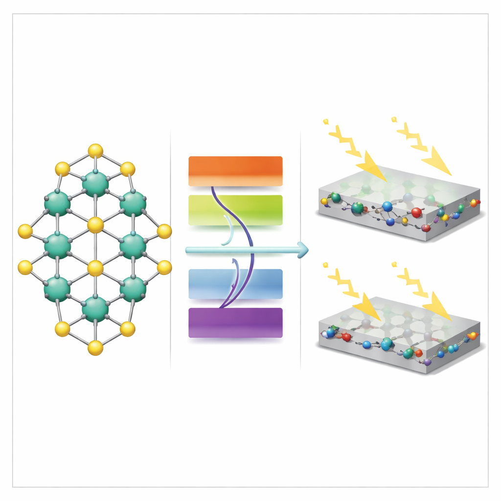
At the heart of this research are crystals with a repeating three-part pattern: a cesium atom (Cs), a transition metal (either niobium, Nb, or vanadium, V), and sulfur (S). The atoms arrange themselves into a framework known as a perovskite, where the metal atoms sit inside sulfur cages and cesium sits between them, helping to hold the structure together. The team used a well-established quantum-mechanical method, density functional theory, to let the atoms "relax" into their most comfortable positions on the computer. They found that both CsNbS3 and CsVS3 fit within the expected size rules for stable perovskites, and that the overall shapes of the two crystals are similar but not identical. Subtle distortions—nearly cube-like for CsNbS3 and more skewed for CsVS3—turn out to matter for how the materials interact with light and electricity.
Electrons on the Edge Between Metal and Semiconductor
To understand whether these compounds behave more like metals or semiconductors, the authors calculated their electronic band structures—essentially maps of where electrons are allowed to exist in energy. Within one common level of theory, both materials show very small indirect band gaps, placing them close to the boundary between a metal and a semiconductor. The top of the filled bands is mostly due to sulfur electrons, while the lowest empty bands are dominated by electrons on the transition metals. This mixing, or hybridization, is a hallmark of chalcogenide perovskites and strongly influences how easily electrons can be excited by light. When the researchers switched to a more sophisticated (hybrid) level of theory, they found that these tiny gaps can shift or even close, producing semi-metal-like features. Rather than taking those numbers at face value, the authors use them to highlight how sensitive such narrow-gap materials are to the details of the calculation.
How Well They Catch and Carry Light
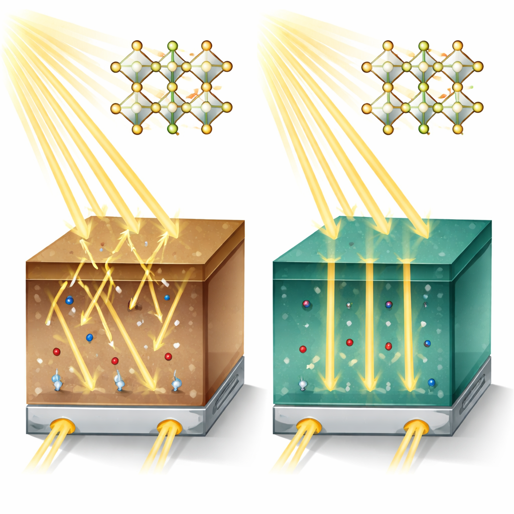
Because solar cells depend on absorbing photons and turning them into moving charges, the team next computed a range of optical properties—how these crystals respond to light across visible and near-infrared energies. Both CsNbS3 and CsVS3 show very strong absorption in the visible and near-infrared ranges, meaning a thin layer can capture a large fraction of incoming sunlight. CsNbS3 behaves more like a narrow-gap semiconductor: it has a clear onset of absorption at low energies and strong peaks tied to specific electronic transitions. CsVS3 looks more metallic or semi-metallic, with light absorption and electrical response that start right from the lowest energies, as if free carriers are already present. Measures such as reflectivity, refractive index, and optical conductivity all reinforce this picture: CsVS3 reflects more and conducts more like a metal at low energies, while CsNbS3 sits closer to the metal–semiconductor divide.
What the Numbers Mean for Solar Devices
To make their findings more practical, the authors plugged the computed absorption data into a model that estimates the best possible efficiency for a solar absorber, known as the spectroscopic limited maximum efficiency. They varied the thickness of the absorbing layer from ultrathin films to a few micrometres. Both materials reached efficiencies in the low-to-mid teens, with CsVS3 around 14% and CsNbS3 around 13% in this idealized scenario. Importantly, the efficiencies rose quickly with thickness and then leveled off, suggesting that only very thin films are needed to harvest light effectively. CsVS3 tends to provide higher current but lower voltage, while CsNbS3 offers higher voltage but slightly lower current, hinting that the two could complement each other in layered or tandem solar designs.
Why This Work Matters
Overall, the study paints a detailed and internally consistent picture of two promising solar materials without over-claiming about real devices. It shows that CsNbS3 and CsVS3 are strong light absorbers with electronic behavior perched between that of metals and classic semiconductors, and that modest thicknesses could be enough for efficient light harvesting. At the same time, the work underscores that for such borderline systems, calculated properties depend strongly on the chosen theoretical approach, and that careful interpretation is essential. Future research that adds vibrational stability checks, finite-temperature effects, and more advanced treatments of electron interactions will be needed to confirm how these materials perform in real-world solar cells and ultraviolet detectors.
Citation: Balogun, R., Aroloye, J.S., Nubi, O.O. et al. Insilico investigations of the physical properties of hexagonal chalcogenide perovskites CsXS3 (X = Nb, V) for UV optoelectronic devices and photovoltaic applications. Sci Rep 16, 14344 (2026). https://doi.org/10.1038/s41598-026-41097-y
Keywords: chalcogenide perovskites, solar cell materials, density functional theory, optoelectronic properties, thin-film photovoltaics