Clear Sky Science · en
A new group of active impedance source inverters with lower components and voltage stress across active switches
Smaller power boxes with less electrical strain
From electric cars to factory robots, many modern machines rely on electronic "power boxes" that turn a steady battery voltage into a controllable, high-voltage waveform. The trouble is that today’s designs often waste space and put heavy electrical stress on their parts, which can shorten lifetime and raise cost. This paper introduces a new family of inverter circuits that can squeeze more usable voltage out of the same source while keeping the internal components cooler and under less strain, all in a more compact package.
Why changing DC into AC is so challenging
Inverters are the devices that convert direct current from batteries or supplies into alternating waveforms suited for motors, heaters, and industrial processes. Traditional designs either only reduce voltage or need an extra stage to boost it, adding bulk and complexity. A popular workaround, called a Z-source inverter, builds a special input network of coils and capacitors that can both raise and shape the voltage in a single stage. However, many such designs suffer from large voltage swings on their parts, interruptions in input current, and a long list of bulky components. These drawbacks matter in real machines, where size, efficiency, and reliability are crucial.
A new way to arrange familiar building blocks
The authors propose five closely related circuit layouts, each based on a simple idea: keep the main power bridge that creates the output waveform, but connect it to an “active impedance” network made from just two coils, two capacitors, two diodes, and one extra switch. By changing where the input source is tied into this network, they obtain five options (named PT1 through PT5) that trade off voltage gain and electrical stress in different ways. A dedicated control method times the switching so that, during special intervals, current circulates within the network to build up energy, and during the rest of the cycle that stored energy is pushed to the output at a higher voltage. This approach avoids extra transformers and keeps the component count low.
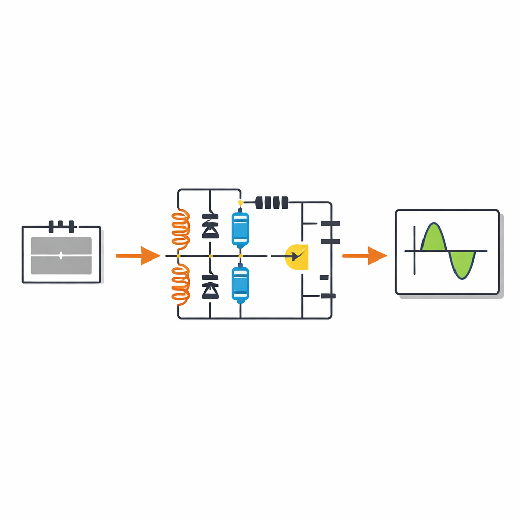
How the control scheme shapes energy flow
To make the new inverters work, the switches must be driven with carefully crafted pulses. The authors develop a pulse-width modulation strategy that uses a triangular carrier waveform and a pair of simple step signals. Logical combinations of these signals determine when each leg of the output bridge conducts normally and when a brief “short” state is allowed so that the active impedance network can charge. By adjusting the fraction of time spent in this special state, known as the duty cycle, the circuit can smoothly tune how much the input voltage is boosted. The team analyzes each operating mode in detail, writing equations for the voltages on coils and capacitors and the currents through all key paths, and from these derive design formulas for choosing component sizes and predicting ripples.
Comparing stress, size, and efficiency
Armed with mathematical expressions for voltage gain and electrical stress, the authors compare their five layouts with a number of well-known alternatives from the research literature. They look at total voltage across capacitors, diodes, and switches, at how strongly the voltage gain depends on the duty cycle, and at how much coil and capacitor volume is needed. In general, the new circuits match or exceed the voltage boosting ability of prior designs while cutting the summed voltage burden on parts, especially in topologies PT3, PT4, and PT5. Because the passive components can be smaller and fewer, the overall power density improves. Simulation-based efficiency tests across a range of power levels show that the first topology, PT1, in particular can reach efficiencies above 90 percent while still using a compact set of parts.
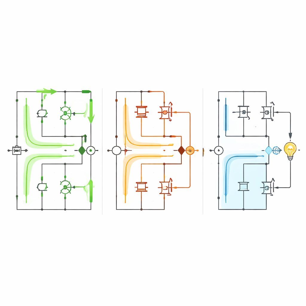
From equations to hardware on the bench
The work goes beyond paper designs. The team builds a physical prototype of the PT1 topology using commonly available coils, capacitors, diodes, and transistors, and implements the control logic on a small microcontroller with gate drivers. Measurements of output voltage, internal capacitor levels, diode and switch stresses, and input and coil currents match the predictions of the analytical model closely, with only small deviations due to real-world losses. Further experiments demonstrate that simply changing the duty cycle allows the output voltage to be adjusted in real time, and that the input current and internal currents remain smooth, which helps limit noise and heating.
What this means for real-world machines
In plain terms, this research shows how to rearrange familiar electronic parts so that inverters can deliver higher, tunable output voltages without beating up their own components or growing in size. The proposed circuits are especially well suited to stand-alone industrial systems, such as electroplating baths and induction heaters, where high-frequency, non-sinusoidal waveforms are acceptable and tight grid standards do not apply. By lowering voltage stress, trimming component count, and maintaining high efficiency, these new inverter families promise more compact, robust, and cost-effective power stages for future industrial equipment.
Citation: Ranjbarizad, V., Babaei, E. & Salahshour, S. A new group of active impedance source inverters with lower components and voltage stress across active switches. Sci Rep 16, 11270 (2026). https://doi.org/10.1038/s41598-026-40820-z
Keywords: power electronics, impedance source inverter, high voltage gain, industrial power conversion, energy-efficient inverters