Clear Sky Science · en
Sputtering-driven formation of interstitial oxygen for intrinsic NIR detection in IGZO phototransistor
Seeing Hidden Light in Everyday Materials
Many of the invisible signals that power modern life—like those used in fiber-optic communication, medical sensors, and food testing—live in the near‑infrared (NIR) part of the spectrum, just beyond red light. Detecting this light usually requires complex, expensive materials. This paper shows how a widely used transparent semiconductor, IGZO, can be gently “re-tuned” during manufacturing to see NIR light on its own, without extra layers or exotic additives. That simplicity could make it far easier and cheaper to build large, sensitive cameras and sensors for uses ranging from quality control in coffee to wearable health monitors.
Turning a Common Film into a Light Sensor
IGZO—short for indium gallium zinc oxide—is already a workhorse material in flat‑panel displays because it conducts electricity well while remaining transparent. But its large internal energy gap means it normally responds only to visible and ultraviolet light, ignoring NIR light that has lower energy. Previous attempts to push IGZO into the NIR have bolted on other components, such as quantum dots or organic dyes, or relied on heavy chemical doping. Those approaches work, but they complicate fabrication, raise costs, and can create unstable interfaces that age poorly in real devices.
Changing the Angle, Not the Recipe
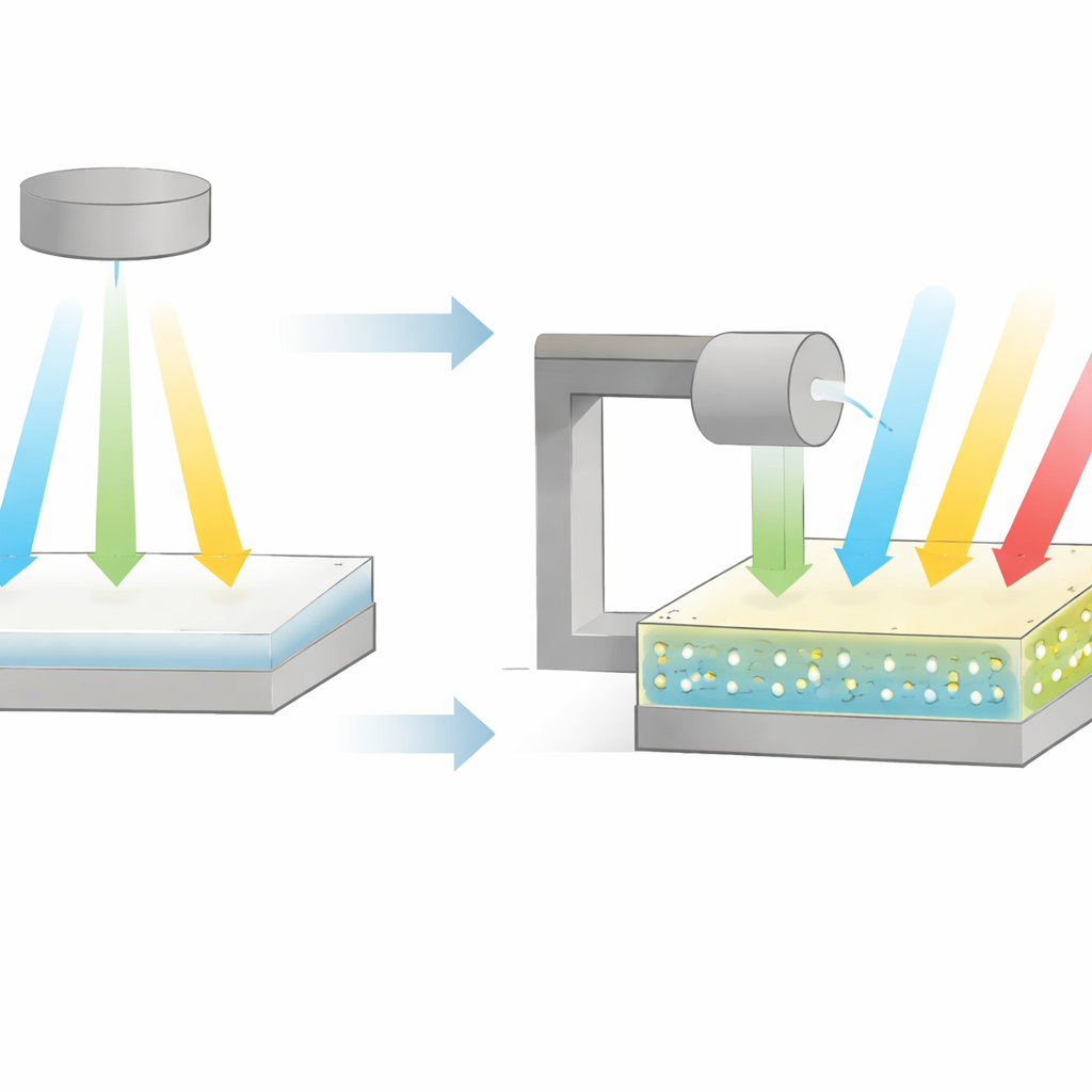
The authors take a strikingly simple route: they keep the IGZO chemistry the same but change how the thin film is deposited. In the standard “on‑axis” sputtering setup, the source material sits directly above the substrate, and energetic particles slam straight into the growing film. In the alternative “off‑axis” configuration, the source is placed to the side so that particles arrive more gently and at an angle. Devices made from on‑axis films behave as expected, reacting only to visible light. In contrast, otherwise identical devices made from off‑axis films suddenly show a strong, repeatable response to NIR light at 850 nanometers, all without adding any extra light‑absorbing layers.
Invisible Oxygen Guests that Shift the Rules
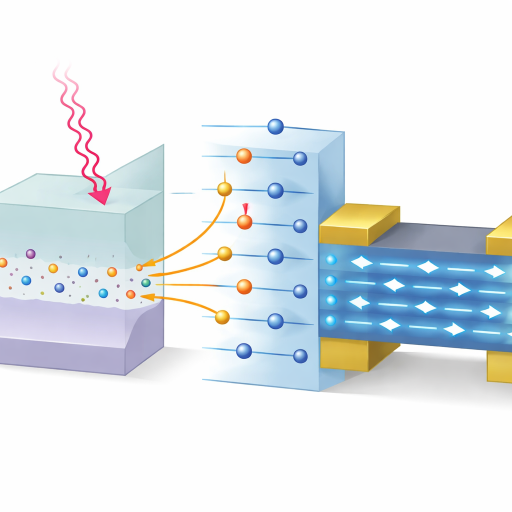
To find out why geometry alone changes the behavior so dramatically, the team probed the films with X‑ray photoelectron spectroscopy, a technique that reveals which types of atoms and bonds are present. Both film types contained nearly the same amounts of indium, gallium, zinc, and oxygen, but the off‑axis films held a small yet distinct population of “interstitial” oxygen atoms—extra oxygen squeezed into spaces within the atomic network rather than locked into the usual lattice positions. Computer simulations using density functional theory showed that these extra oxygen atoms create new energy levels just above the film’s valence band, only about 0.1 to 0.5 electron volts higher. These shallow states effectively shrink the energy gap that incoming light must bridge, letting NIR photons be absorbed where they otherwise would pass through.
How the New States Boost the Signal
When NIR light shines on the off‑axis IGZO transistor, electrons in these shallow oxygen‑related states are nudged into higher‑lying states and eventually influence the channel that carries current between the device’s source and drain contacts. Instead of behaving like a simple on‑off switch, the device acts more like a light‑controlled gate: charges trapped in the shallow states modulate the electric field in the channel, a process known as photogating. This mechanism naturally amplifies the current response, yielding a very high responsivity and detectivity compared with many IGZO‑based NIR detectors that rely on added sensitizers. The trade‑off is a slower fall time as trapped charges leak back, but the devices remain stable over repeated cycles and over days of storage in air.
From Lab Light to Coffee Cups
To illustrate real‑world potential, the researchers used their NIR‑sensitive IGZO devices to estimate sugar content in brewed coffee. NIR light can penetrate dark liquids where visible light is strongly absorbed, making it ideal for this task. The off‑axis devices produced clear, progressively larger photocurrents as more sugar was dissolved into the coffee, and the calculated sugar levels closely matched those from a commercial refractometer—especially at high concentrations where the standard instrument struggled. Because the sputtering‑angle method is simple, repeatable, and compatible with existing chip fabrication, it could be scaled up to large sensor arrays for food monitoring, imaging, or integrated optical circuits.
Simple Process, Broad New Possibilities
In everyday terms, the work shows that you can teach a familiar material a new optical trick by changing how you “spray paint” it onto a surface, rather than by altering the paint itself. By slightly tilting the sputtering source, the authors stabilize tiny pockets of extra oxygen inside IGZO that act as stepping stones for electrons under NIR light. This built‑in pathway allows the film to sense wavelengths it normally ignores, turning a standard display material into a broadband light detector without added complexity. Such geometry‑driven defect engineering offers a practical, low‑cost way to build sensitive, large‑area NIR sensors that fit smoothly into conventional electronics manufacturing.
Citation: Choe, J., Bong, H., Lee, H. et al. Sputtering-driven formation of interstitial oxygen for intrinsic NIR detection in IGZO phototransistor. Sci Rep 16, 11065 (2026). https://doi.org/10.1038/s41598-026-40769-z
Keywords: near infrared photodetector, IGZO transistor, thin film sputtering, defect engineering, noninvasive sensing