Clear Sky Science · en
Effect of initial stress on electro-magneto-thermoelastic semiconductor materials exposed to a pulsed lasers due to the interaction between electrons and holes
Light, Heat, and Stress Inside Everyday Chips
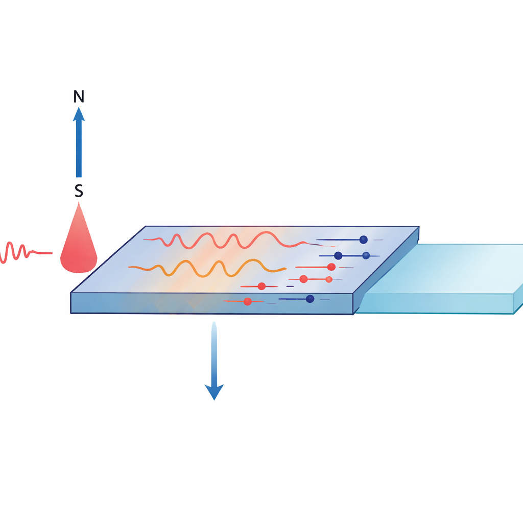
From smartphones to solar panels, silicon chips quietly endure bursts of light, heat, magnetic fields, and internal strain as they operate. This paper explores what happens deep inside such a semiconductor when a short laser pulse strikes it while a magnetic field is applied and the material is already under mechanical stress. Understanding these hidden interactions helps engineers design faster, safer, and more reliable electronic and sensing devices.
How Electrons, Holes, and Heat Move Together
In a semiconductor like silicon, electric current is carried not only by electrons but also by “holes,” which act as positively charged partners. When a laser pulse hits the surface, it suddenly heats the material and creates extra electrons and holes. At the same time, a magnetic field bends their motion, producing what is known as Hall current. The study looks at how heat, moving charges, and mechanical deformation influence one another, rather than treating them as separate effects. The author builds a unified mathematical model that links temperature, stress, and the densities of electrons and holes in a single framework.
Building a Unified Wave Model in Silicon
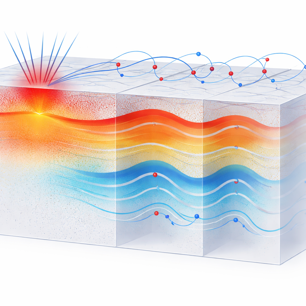
The work focuses on waves that travel inside a semi-infinite block of silicon—essentially a half-space representing a thick chip. When the laser pulse deposits energy at the surface, it launches a complex family of waves: thermal waves that carry heat, elastic waves that carry mechanical stress and displacement, and plasma-like waves associated with electrons and holes. To handle this, the author uses a technique called normal mode analysis, which represents each physical quantity as a wave with a certain frequency and spatial pattern. This allows the coupled equations that describe temperature, stresses, and carrier motion to be solved in an analytical form, under carefully chosen boundary conditions that mimic a rigid, illuminated surface and a quiet interior where disturbances vanish far from the surface.
Role of Pre-Stress, Magnetic Fields, and Laser Pulses
Armed with the analytical solutions, the author then turns to numerical simulations for silicon using realistic material constants. The results show how several key knobs—initial mechanical stress, the strength of the magnetic field (through the Hall current), and the properties of the laser pulse—reshape the internal fields. Increasing the initial stress tends to raise the temperature, displacement, and normal stress near the surface, while reducing the shear stress. When the magnetic field is strong enough to generate a Hall current, the variations in temperature, carrier density, and normal stress become smaller and decay more quickly with depth, meaning the disturbance is more tightly confined near the surface. Similarly, the presence of a laser pulse modifies how sharply these quantities rise and then fade, highlighting how sensitive mechanical and thermal waves are to the timing and shape of the optical excitation.
Comparing Competing Theories of Heat and Stress
The study also compares three widely used thermoelastic theories, which differ in how they account for finite speeds and delays in heat transport and stress response. Under the same conditions, each theory predicts a different pattern for temperature, carrier density, hole concentration, and normal stress as a function of depth. The results indicate a consistent ordering of the response strengths across the models, emphasizing that the choice of theory can significantly affect predicted wave amplitudes and decay rates. This comparison is important for researchers who use such models to interpret experiments or to design devices where short laser pulses and strong fields are involved.
Why These Hidden Waves Matter
Overall, the paper shows that pre-existing mechanical stress, magnetic fields, and laser pulses jointly control how heat, charge carriers, and elastic waves move inside semiconductors. Even small changes in initial stress or pulse timing can noticeably alter temperature peaks, carrier distributions, and stress profiles over short distances from the illuminated surface. These insights are valuable for technologies that rely on precise control of heat and stress in active materials, from photo-thermoelastic sensors and Hall-based magnetic detectors to advanced medical instruments and components in electric vehicles. By tying together thermal, electrical, and mechanical effects in a single model, the work offers a more complete picture of how real semiconductor devices respond under demanding operating conditions.
Citation: Alarfaj, K.K. Effect of initial stress on electro-magneto-thermoelastic semiconductor materials exposed to a pulsed lasers due to the interaction between electrons and holes. Sci Rep 16, 11630 (2026). https://doi.org/10.1038/s41598-026-37940-x
Keywords: semiconductor thermoelasticity, laser pulse interaction, Hall effect, magnetoelastic waves, silicon stress waves