Clear Sky Science · en
Multimodal electron microscopy of halide perovskite interfacial dynamics
Why your next smart screen may depend on this
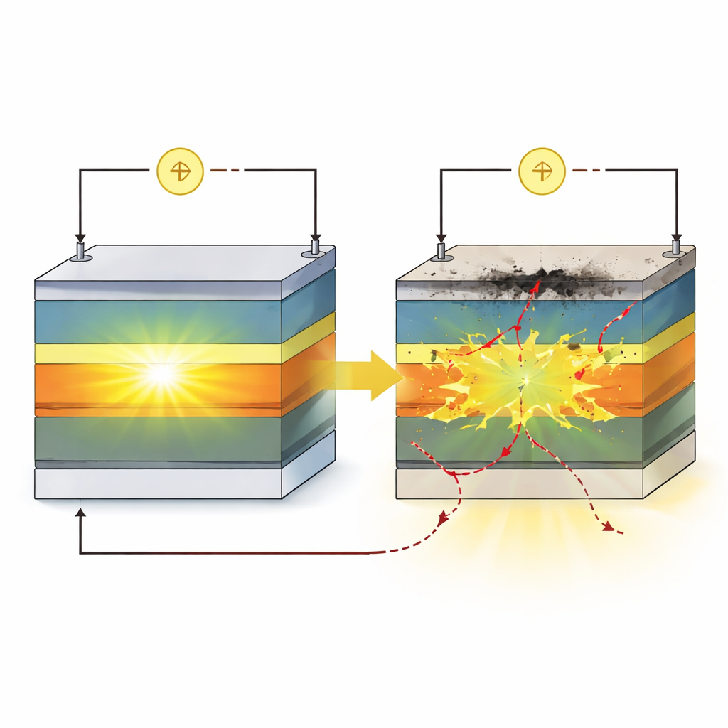
From ultra-bright phone displays to vivid TVs, a new class of materials called halide perovskites could make future screens cheaper, more colorful and more energy efficient. Yet these promising light-emitting diodes (LEDs) currently burn out in minutes rather than years. This study peers inside a working perovskite LED at the level of individual atoms, revealing exactly where and how the device falls apart—and what engineers must fix to make these lights last.
Peeking inside a tiny blue light
The researchers focus on sky‑blue perovskite LEDs, which use solution‑processed crystals to produce light when an electric current flows. Instead of looking only at the overall brightness or electrical behavior, they carve out an ultrathin cross‑section of a real device and wire it onto a microscopic chip so it can be switched on inside an electron microscope. Using a combination of imaging modes, they simultaneously track the crystal structure, the distribution of elements and the device’s electrical response as it operates, achieving nanometer‑scale detail while the LED is actually working.
Stress at the borders, calm in the middle
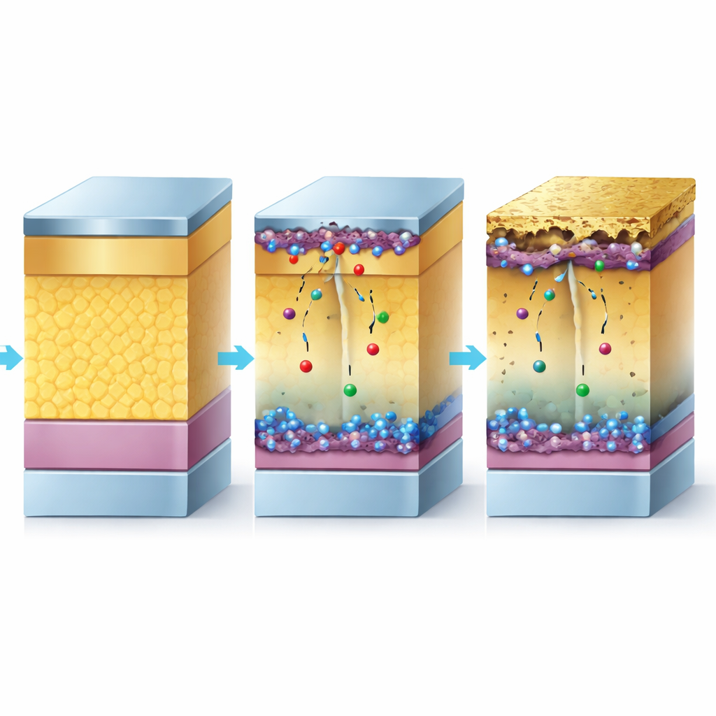
Before the device is driven hard, the central perovskite layer looks like an orderly crystal, while the regions where it touches neighboring transport layers already show subtle disorder. Atomic‑scale maps of lattice strain—how much the crystal spacing stretches or compresses—reveal pockets of built‑in stress and tiny regions enriched in lead at these interfaces. The bulk of the perovskite remains largely strain‑free, but at the borders with the surrounding organic layers the crystal is slightly misaligned and peppered with secondary lead‑rich phases. These “weak seams” are present from the start and turn out to be the places where damage accelerates once current is applied.
Watching damage spread under real operating conditions
The team then runs the nano‑LED at a constant current similar to that used in full devices, taking snapshots after several minutes of operation. As time passes, the voltage needed to maintain the same current rises sharply, signaling that the device is becoming more resistive. Diffraction patterns from the perovskite show that its lattice first distorts and then partially collapses, and new signatures of lead‑rich compounds and metallic lead itself appear. Real‑space images confirm grain fragmentation, loss of material, and clustering of heavy lead‑based regions, particularly near the interfaces. Despite this, large portions of the perovskite interior keep their original structure, indicating that the main light‑emitting sites survive while pathways for charges to reach them are being choked off.
Corroding contacts and traveling ions
One of the most striking findings is what happens to the metal electrode that injects electrons. Under bias, chloride ions from the mixed bromide–chloride perovskite migrate toward the aluminum contact. There they react to form a new, insulating aluminum chloride layer that thickens with continued operation. This extra layer blocks electrons, forces the device to run at higher voltage and likely causes local overheating. At the same time, halide ions rearrange within the perovskite, leaving behind regions enriched in lead‑based by‑products at both the top and bottom interfaces. These lead‑rich phases act as traps that kill light emission and further disrupt the crystal, turning the perovskite stack into a tiny, unintended electrochemical cell where the interfaces slowly corrode.
Rethinking how to make perovskite lights last
By directly watching a working perovskite LED fall apart layer by layer, this study shows that the device’s short lifetime is not mainly due to the light‑emitting bulk material losing its ability to glow. Instead, the Achilles’ heel lies at the buried borders between layers and at the metal contact, where strain, ion motion and chemical reactions combine to break electrical connectivity. The authors argue that stabilizing these interfaces—by reducing built‑in strain, slowing or blocking ion migration, and protecting metal contacts from halide attack—should dramatically extend device lifetimes. Their multimodal electron microscopy approach also provides a general roadmap for diagnosing failure in other complex thin‑film optoelectronic devices, bringing long‑lived perovskite displays and lighting a step closer to reality.
Citation: Li, X., Gu, Q., Huang, W. et al. Multimodal electron microscopy of halide perovskite interfacial dynamics. Nature 651, 614–620 (2026). https://doi.org/10.1038/s41586-026-10238-8
Keywords: perovskite LEDs, device degradation, interfacial chemistry, electron microscopy, ion migration