Clear Sky Science · en
Nanophotonic waveguide chip-to-world beam scanning
Bringing Light Safely Off the Chip
Much of modern life runs on light moving through tiny glass or silicon highways inside data centers, phones and future quantum computers. But the real world that cameras see, cars navigate and microscopes probe is made of light flying freely through space. This paper describes a new kind of chip device, nicknamed a “photonic ski-jump,” that lets a computer chip launch and rapidly steer a razor-sharp beam of light out into the open world. That ability could power smaller LiDAR for self-driving cars, lighter augmented-reality displays, faster 3D printers and scalable control of quantum bits of information.
From Glass Threads to Open Air
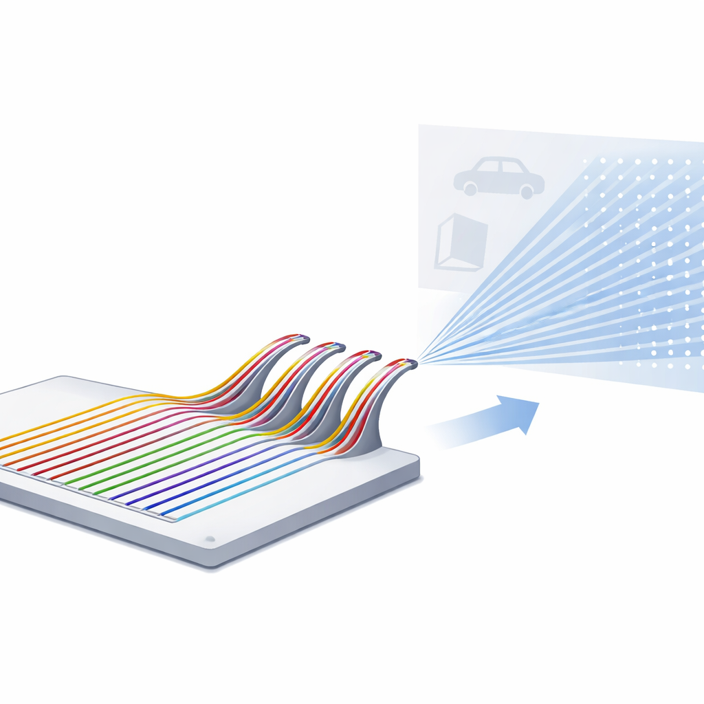
Today’s optical chips are extremely good at shaping and timing light as it travels inside microscopic waveguides—essentially glassy wires for photons. The outside world, however, offers an enormous number of directions and positions that light can take, like pixels on an ultra-high-resolution screen. Bridging these two realms has been hard. Existing chip-based beam steering devices can address many directions but smear out the beam, while tiny mechanical mirrors give beautiful beams but are bulky and slow to move. The authors argue that the key is an interface that can send a single, clean, diffraction-limited beam from anywhere on a chip to a very large number of spots in space, and do so quickly from a very small footprint.
A Tiny Ramp That Throws Light
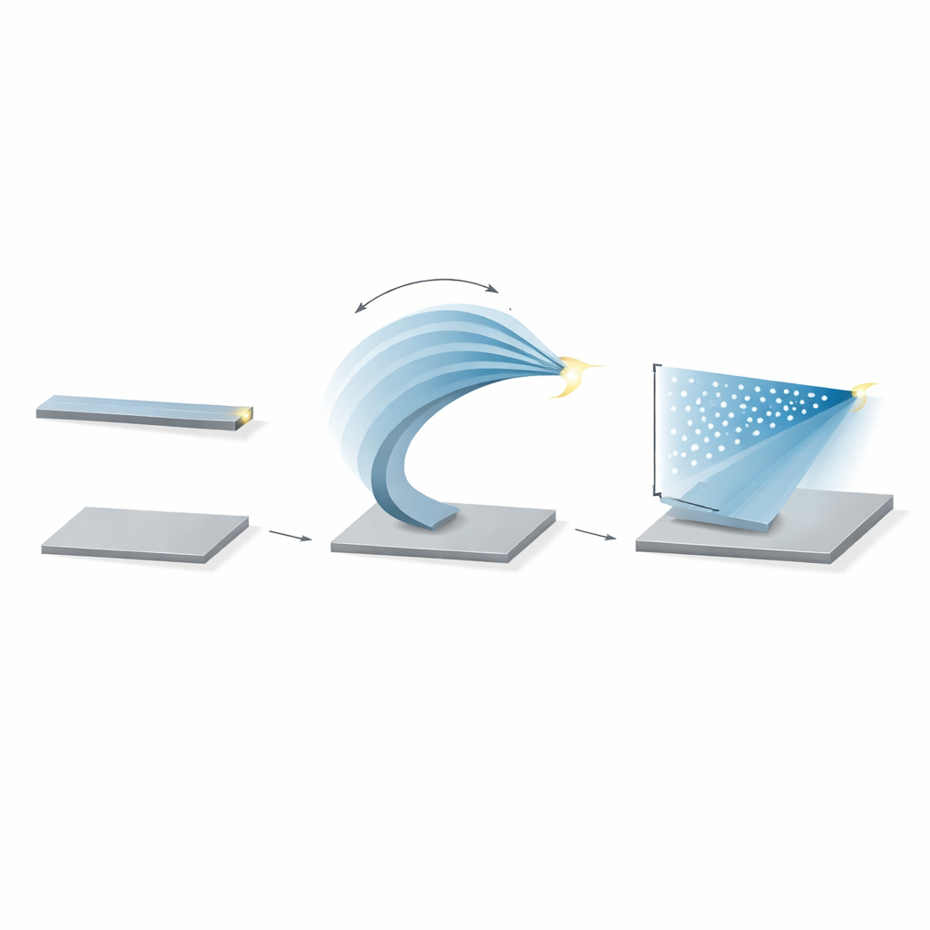
Their solution is to build a microscopic ramp on the chip. This “ski-jump” is a thin, curved cantilever—only about 2 micrometres thick—with an optical waveguide running along its top. The cantilever is made from layers of standard semiconductor materials whose built-in stresses cause it to curl gently upward when released, lifting the waveguide out of the chip plane by tens to hundreds of micrometres. At the curled tip, the waveguide narrows so the light exits as a tiny, bright beam less than a micrometre wide, close to the physical limit for sharpness. Because the structure is so light, a piezoelectric layer can wiggle it at kilohertz to hundred-kilohertz rates using modest voltages, sweeping the beam rapidly across space like a super-fast flashlight.
Painting with Light at High Speed
By carefully choosing how they drive the tiny ramp, the researchers can scan the beam in one or two dimensions. Driving the main bending direction makes the tip trace an arc; adding sideways motion with a split electrode produces Lissajous patterns—loops that slowly fill up a rectangular field of view. When combined with pulsed lasers of different colors, the ski-jump draws full-color images and even videos onto a screen, all from a device occupying less than a tenth of a square millimetre. The team defines a simple performance score: how many distinct beam spots per second can be addressed per square millimetre of device area. Their ski-jump reaches tens of millions of spots per second per square millimetre, more than fifty times better than leading tiny mirrors and a thousand times better than previous scanning fibers, yet it is made in a standard CMOS factory.
Reaching Down to Single Quantum Emitters
Beyond displays and ranging, the authors show that the same device can delicately control individual quantum light sources. They shine the ski-jump’s beam into a small diamond chip that hosts artificial atoms known as silicon vacancy centers, cooled to a few degrees above absolute zero. By scanning the beam along one line, they repeatedly excite a single center and detect the stream of single photons it emits, confirming that only one emitter is being addressed at a time. They also sweep across multiple nearby waveguides in the diamond, lighting up different groups of emitters in sequence. This suggests a path to steering light to thousands or millions of quantum bits packed on a chip, something that would be unwieldy using traditional bulk optics.
Scaling Up to Billions of Light Points
The team analyzes how to scale from one ski-jump to dense arrays across an entire wafer. Because the devices are made with standard processes, they can place dozens or hundreds on a single chip and show that their shapes are uniform to within a few percent. Paired with compact lenses similar to those found in smartphone cameras, these arrays could project or collect light from more than a billion resolvable points at kilohertz refresh rates within a palm-sized module. Remaining engineering challenges—such as packaging the devices in small vacuum enclosures and compensating for the natural curved scan paths—are important but, the authors argue, manageable with existing techniques.
What This Means for Everyday Technology
In plain terms, this work turns an optical chip into a kind of solid-state “light engine” that can both understand and affect the world around it. A single platform can route light on-chip for fast processing, then fling it outward as a sharp, steerable beam to scan a room for a car, draw an image on your retina, etch features in a 3D printer or tickle individual quantum bits. By breaking long-standing trade-offs between beam quality, speed and size, the photonic ski-jump offers a practical route to machines that see and communicate with unprecedented detail, while keeping the hardware compact and manufacturable at scale.
Citation: Saha, M., Wen, Y.H., Greenspon, A.S. et al. Nanophotonic waveguide chip-to-world beam scanning. Nature 651, 356–363 (2026). https://doi.org/10.1038/s41586-025-10038-6
Keywords: nanophotonics, beam scanning, integrated photonics, LiDAR, quantum optics