Clear Sky Science · en
Predicting temperature-dependent optoelectronic properties of semiconductor defects with equivariant neural networks
Why tiny flaws in crystals matter
Modern electronics and solar cells are built from nearly perfect crystals, yet their performance is often dictated by tiny imperfections called defects. These flaws can trap charge, leak energy as heat or light, and change how a device behaves as it warms up. This article shows how advanced neural networks can track what these defects do at realistic temperatures without the huge computing costs that have limited such studies until now. 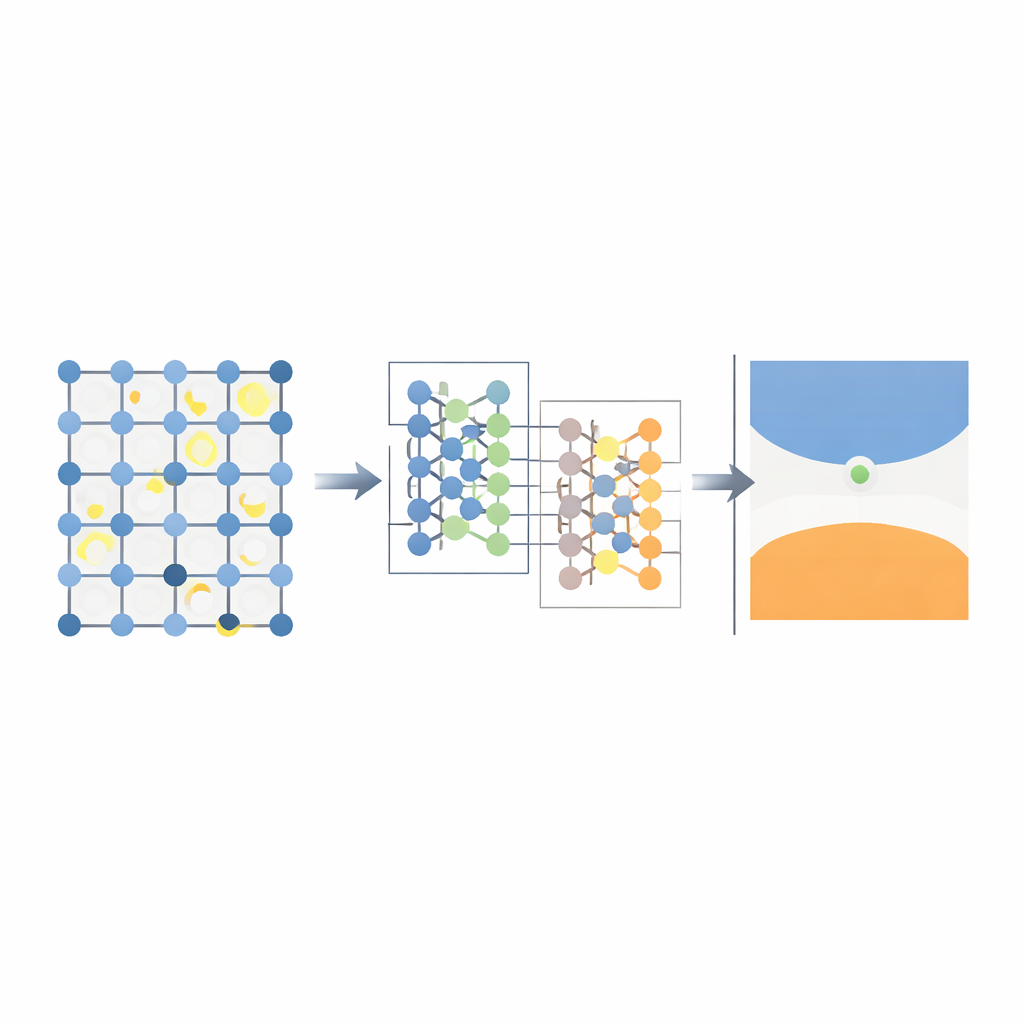
The challenge of seeing hidden troublemakers
Defects in semiconductors like gallium arsenide are crucial for both good and bad reasons. Some are deliberately introduced to tune conductivity, while others quietly sap efficiency in LEDs and solar cells. To understand them, researchers normally rely on quantum mechanical simulations that treat electrons explicitly. However, these calculations become extremely demanding when the simulated crystal must be large enough to isolate a single defect and when thermal vibrations at operating temperatures are included through molecular dynamics. As a result, accurate temperature dependent predictions have been out of reach for many practically important defects.
Teaching neural networks the rules of atoms
The authors tackle this by combining two special graph based neural networks that are built to respect the symmetries of three dimensional space. One network, MACE, learns how atoms push and pull on each other so it can replace costly quantum based dynamics with a machine learned force field. The other, called DeepH, learns the electronic Hamiltonian, the mathematical object from which energies and band structures are obtained. An active learning strategy ties them together: the models are trained first on a small set of carefully chosen quantum calculations, then iteratively improved by asking where their own predictions are most uncertain and adding just those challenging cases to the training data.
Putting defects in gallium arsenide under the microscope
To test their framework, the researchers focus on five common point defects in gallium arsenide, a key material for high quality lasers and solar cells. They show that the MACE force field reproduces atomic vibrations and local structures around defects with accuracy close to full quantum simulations, but at far lower cost. DeepH then takes snapshots from these machine learned trajectories and predicts the electronic band structure, including the special levels introduced by defects inside the band gap. Across a range of temperatures and system sizes, the learned Hamiltonian tracks conventional calculations to within only a few tens of millielectronvolts, while running more than thirty times faster for large supercells.
Following defect levels as the crystal heats up
With both speed and accuracy in hand, the team explores how temperature reshapes the electronic landscape. For pristine gallium arsenide and for crystals containing an arsenic interstitial, the learned model correctly captures the gradual shrinking of the band gap as atoms vibrate more strongly. It also reveals how the energy of the defect level shifts and broadens, reflecting its coupling to thermal motion and the constant reshuffling of the local environment. For the technologically important arsenic antisite defect, which creates a state deep inside the band gap, the approach shows that rising temperature moves this level closer to the conduction band edge and increases its spread, offering quantities that can be compared directly with temperature dependent optical measurements. 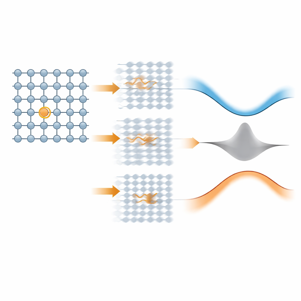
What this means for future devices
In simple terms, this work shows that carefully designed neural networks can learn both how atoms move and how electrons respond in imperfect semiconductors as they heat up. Once trained, the models turn what would be months of heavy computation into calculations that fit within typical computing budgets, without sacrificing the essential physics. This opens the door to routine studies of how defects influence the efficiency and stability of real devices, and offers a template for extending the same strategy to more complex materials, charged defects, and other properties that matter for next generation electronics and solar technologies.
Citation: Zhu, X., Rinke, P. & Egger, D.A. Predicting temperature-dependent optoelectronic properties of semiconductor defects with equivariant neural networks. npj Comput Mater 12, 176 (2026). https://doi.org/10.1038/s41524-026-02111-z
Keywords: semiconductor defects, gallium arsenide, machine learning, neural networks, electronic structure