Clear Sky Science · en
Photoinduced ultrafast charge transfer and enhanced optoelectronics in MoS2/Ti2CO2 van der Waals heterojunction
Turning Thin Materials into Better Solar Engines
Imagine solar cells and light sensors made from sheets of material so thin they are only a few atoms thick. These ultra-thin films can bend, stretch, and stack like high-tech Lego bricks, opening the door to flexible phones, window-integrated solar panels, and tiny optical chips. This paper explores a new stacked pair of such sheets—made from MoS2 and a material called Ti2CO2—that promises to move electric charges with remarkable speed, a key requirement for next‑generation clean-energy and optoelectronic devices. 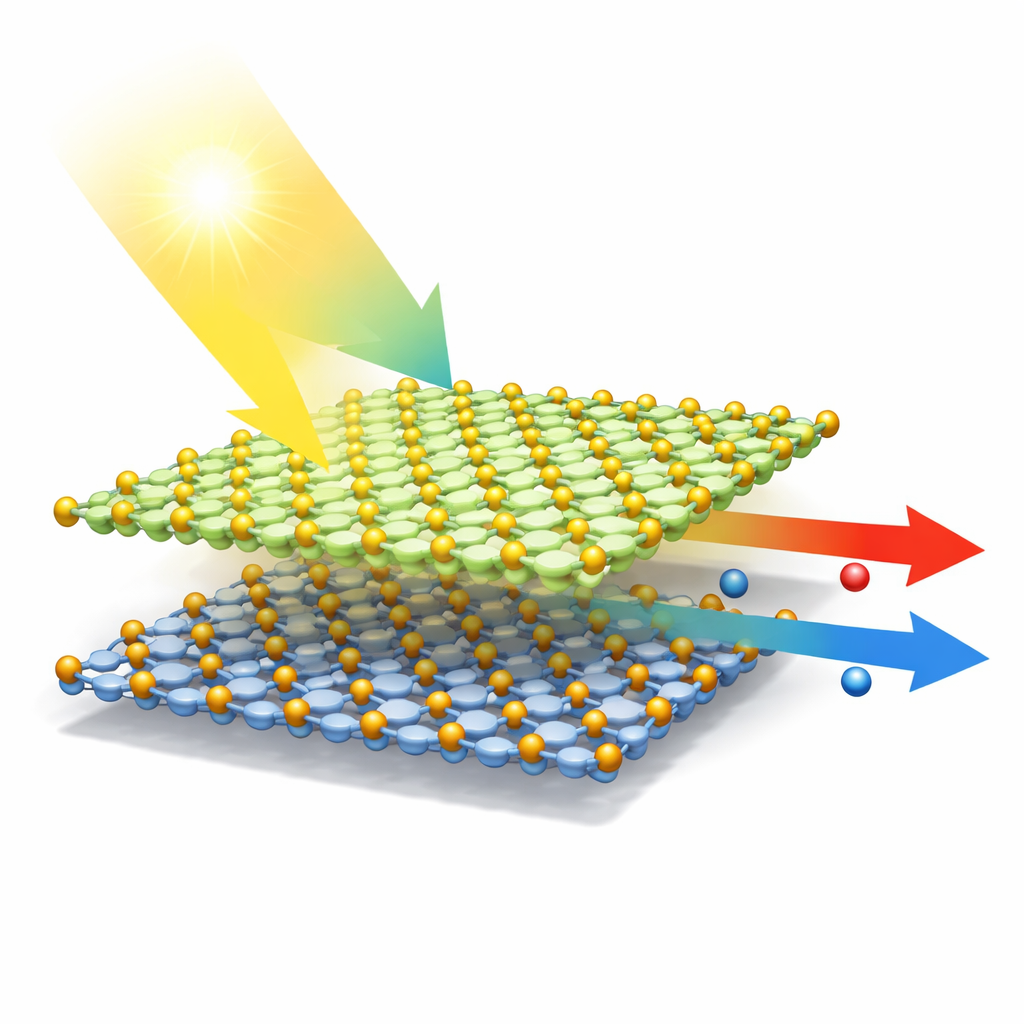
Why Stacking Atom-Thin Layers Matters
Single ultra-thin materials often absorb light well but are simply too thin to grab enough sunlight on their own. By stacking different two-dimensional layers on top of each other, scientists can create “heterojunctions” where the interface between the layers does most of the work. In this study, the authors combine MoS2, a well-known light-absorbing semiconductor, with Ti2CO2, an emerging member of the MXene family that offers strong visible-light absorption and high charge mobility. Together, they form a carefully arranged interface where incoming light generates charges that can be efficiently separated instead of quickly cancelling each other out as heat.
Building a Stable and Helpful Atomic Interface
Using quantum-mechanical simulations, the team first tested many different ways the two sheets could sit on top of one another, looking for an arrangement that is both stable and electronically favorable. They found a particular stacking pattern in which the two lattices fit well enough to lock together through weak van der Waals forces, without forming damaging chemical bonds. In this configuration, the energy levels of the two materials naturally line up in what is known as a “type‑II” pattern: electrons are most comfortable in one layer, while the positively charged “holes” prefer the other. This built-in preference creates a gentle internal electric field across the interface, encouraging electrons and holes to move apart after light hits the material.
Ultrafast Charge Motion Inside the Stack
To see how quickly these charges actually move, the researchers went beyond static pictures and ran non‑adiabatic molecular dynamics—essentially watching how electrons respond in real time to atomic vibrations after a burst of light. They found that electrons jump from MoS2 into Ti2CO2 in only about 4.6 femtoseconds (quadrillionths of a second), while holes drift the opposite way in a few hundred femtoseconds. Once separated, electrons and holes survive for roughly 1.53 nanoseconds before recombining—almost ten times longer than in bare MoS2. Vibrations of the atomic lattice, both slow and fast, help strengthen the coupling between states and speed up electron motion, while the energy spacing between levels slows holes somewhat. Together, these effects create a powerful combination: lightning-fast separation followed by relatively long-lived carriers, ideal for converting light into electricity. 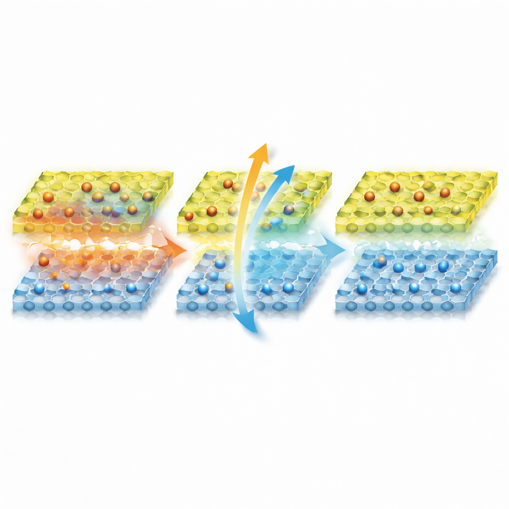
Capturing More Sunlight and Tuning It on Demand
The MoS2/Ti2CO2 pair also turns out to be an excellent light sponge. Compared with pure MoS2, the stacked structure absorbs over a much wider range, spanning most of the visible and part of the ultraviolet spectrum. The team further shows that gently stretching or compressing the layers—what they call biaxial strain—lets them fine-tune the energy gap and how strongly the material absorbs different colors. Under the right conditions, the simulated device could reach a power conversion efficiency of about 12.9%, competitive with other cutting-edge two-dimensional solar absorbers. Beyond photovoltaics, the same interface improves the energetics for important chemical reactions, making the stack a promising candidate for speeding up the production of hydrogen fuel and oxygen in water-splitting systems.
From Theory to Future Devices
Although this work is entirely computational, it builds on fabrication techniques that already exist for both MoS2 and MXenes, and even for related stacked structures. The results provide a kind of design map: choose a stacking pattern that produces type‑II alignment, maintain clean and well-controlled surfaces, and apply mechanical strain as a fine-tuning knob. For non-specialists, the key takeaway is that carefully engineered stacks of atom-thin materials can separate light-generated charges almost instantaneously and keep them apart long enough to do useful work. The MoS2/Ti2CO2 heterojunction showcased here is a clear example, pointing toward flexible, efficient, and potentially low-cost devices for harvesting sunlight and driving clean chemical reactions.
Citation: Yue, X., Zhou, Z., Wang, X. et al. Photoinduced ultrafast charge transfer and enhanced optoelectronics in MoS2/Ti2CO2 van der Waals heterojunction. npj Comput Mater 12, 173 (2026). https://doi.org/10.1038/s41524-026-02035-8
Keywords: two-dimensional materials, van der Waals heterostructures, optoelectronics, solar energy conversion, MXene