Clear Sky Science · en
Revealing the hidden third dimension of point defects in two-dimensional MXenes
Why tiny flaws in flat materials matter
From faster electronics to cleaner water and better batteries, many future technologies will rely on ultrathin materials just a few atoms thick. In these sheet-like substances, even a single missing atom—a point defect—can dramatically change how the material behaves. Yet in real devices these sheets are often stacked in several layers, making it extremely hard to see how such tiny flaws are arranged in three dimensions. This study shows how scientists can finally uncover the hidden 3D landscape of these defects in a promising family of materials called MXenes, opening the door to deliberately “engineering” flaws to tune performance.
Peeking beneath the surface of MXene sheets
MXenes are atomically thin layers of metal and carbon or nitrogen that have attracted intense interest for energy storage, electronics, water purification, and biomedical uses. They are typically made by chemically carving out certain elements from a bulk crystal, a harsh process that also knocks out metal atoms and leaves behind empty sites. Researchers know that these vacancies can strongly affect properties such as conductivity and mechanical strength, but existing microscopes mostly provide flat, top-down images. That means scientists have been largely blind to how defects are arranged across multiple atomic layers inside a single flake, a missing piece that makes it difficult to connect processing conditions to real performance.
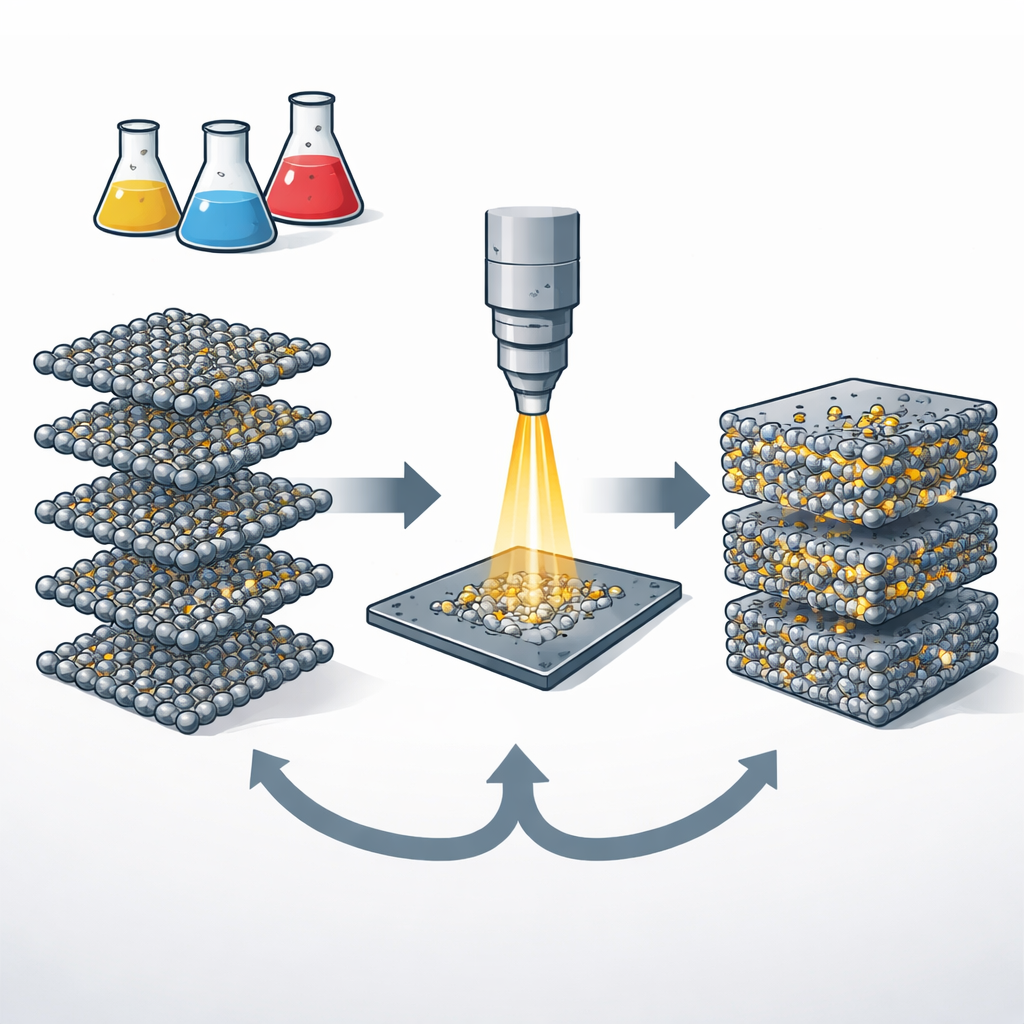
Letting artificial intelligence read atom-by-atom images
To overcome this challenge, the authors developed an artificial intelligence–guided workflow that works hand in hand with advanced electron microscopy. They used a scanning transmission electron microscope to image single flakes of a titanium-based MXene (Ti₃C₂Tₓ) under carefully controlled low-damage conditions. Then, instead of manually marking every atom and missing atom by eye—a slow and error-prone task—they trained two neural networks: one to capture the regular atomic lattice and another to spot vacancies. This approach automatically identified more than 150,000 atoms and about 3,000 vacancies across the three metal layers of many MXene flakes, providing a statistically powerful picture of where defects appear.
Reconstructing the hidden third dimension
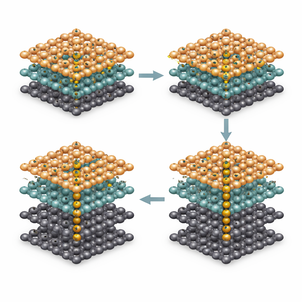
Armed with precise coordinates for each atom and vacancy, the team reconstructed how defects are distributed through the thickness of the MXene sheets. By exploiting the known crystal geometry and the viewing angle in the microscope, they could separate atoms into two outer layers and one middle layer. They found that the outer layers consistently hosted more vacancies than the middle layer, in line with earlier predictions that it is easier to remove atoms from surfaces than from the interior. By comparing samples etched with different strengths of hydrofluoric acid, they showed that harsher conditions not only increase the overall number of missing titanium atoms but also boost the number of defects in subsurface layers.
From lone vacancies to tiny tunnels
The real power of the 3D reconstruction was the ability to classify how vacancies group together. The researchers found four main types: truly isolated missing atoms; surface clusters confined to one layer; inter-layer clusters that link vacancies across neighboring layers; and nanopores, where a vertical chain of missing atoms forms a tiny tunnel through all three layers. Across all samples, nearly half of the defects were part of clusters rather than being isolated. Stronger etching created more of these complex, multi-layer defects and nanopores, although the typical size of each cluster stayed about the same. This suggests that processing conditions mainly change how often such clusters appear, not how big they grow.
Simulations that explain why clusters form
To understand why vacancies prefer to cluster, the team combined their experimental findings with large-scale computer simulations that mimicked the MXene lattice under different hidden conditions, such as the number of missing carbon atoms and the coverage of surface groups attached to the outer metal layers. These simulations showed that when carbon vacancies are more common, titanium vacancies tend to gather nearby, reducing the number of broken bonds and lowering the overall energy. Increasing the density of surface groups, in contrast, makes it less favorable for vacancies to concentrate at the outer layers and pushes some clusters inward. When the researchers matched their simulated defect patterns to the measurements, the best agreement came from scenarios with substantial carbon vacancies and moderate surface coverage, highlighting how these “invisible” ingredients steer the 3D defect landscape.
Designing better materials by tuning their flaws
Altogether, this work demonstrates a new way to see and quantify individual atomic defects throughout the volume of stacked 2D materials, rather than just at the surface. For MXenes, the method reveals how acid strength and related chemistry control whether missing atoms remain isolated or assemble into clusters and nanopores that can strongly influence electrical, mechanical, and chemical behavior. More broadly, the framework of AI-guided microscopy combined with simulation could be adapted to many other layered materials. By turning hidden defect patterns into something that can be measured, classified, and modeled, scientists can begin to design and control “defect topologies” on purpose—tailoring tiny imperfections to build better batteries, catalysts, sensors, and beyond.
Citation: Guinan, G., Smeaton, M.A., Wyatt, B.C. et al. Revealing the hidden third dimension of point defects in two-dimensional MXenes. Nat Commun 17, 3473 (2026). https://doi.org/10.1038/s41467-026-71670-y
Keywords: MXenes, point defects, electron microscopy, machine learning, 2D materials