Clear Sky Science · en
Capacitive piezotronics
Feeling the pressure in tiny electronics
Our phones, sensors and wireless gadgets all rely on clean, fast electrical signals. But as these devices shrink to the nanoscale, even the thinnest boundary inside a material can disturb how signals travel. This study shows how gentle mechanical pressure, such as squeezing or bending a device, can be used to fine tune those invisible boundaries and improve how high frequency signals are handled, opening a path toward smarter and more responsive communication hardware.
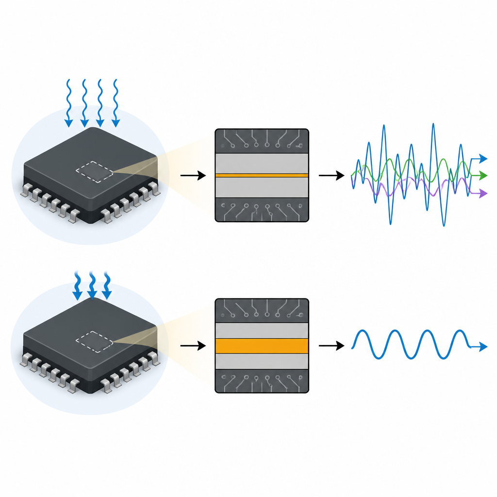
A new way to control tiny borders
At the heart of many electronic components lies a junction, a narrow region where a metal meets a semiconductor. Traditionally, engineers have learned to control these junctions by changing how high an energy barrier is, which affects how easily electrical charges can flow in one direction. This approach powers a field known as piezotronics, where mechanical strain in special crystals creates internal electric charges that raise or lower this barrier and change a device’s resistance. However, another equally important property of the junction, its physical width, has been largely overlooked, especially when the device handles rapidly alternating signals instead of steady currents.
Turning pressure into tunable capacitance
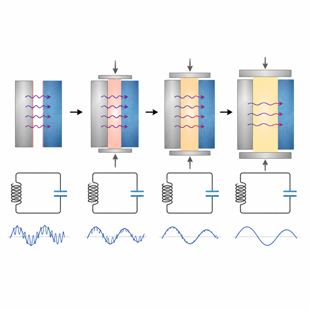
The authors introduce “capacitive piezotronics,” a concept where mechanical strain is used not to change how tall the barrier is, but how thick the junction region becomes. In certain crystals such as gallium nitride and zinc oxide, squeezing or stretching along a preferred axis produces built in electric charges. These charges push or pull mobile electrons and holes near the junction, effectively widening or narrowing the depleted region where few free charges exist. Because the electrical capacitance of the junction depends directly on that width, strain provides a reversible knob to raise or lower capacitance while the device carries high frequency alternating signals.
Probing single and dual junction devices
To test this idea, the team built simple devices that sandwich a piezoelectric semiconductor between metal contacts, forming one or two junctions in series. They measured how capacitance changed as they gently pressed along the crystal’s polar axis while applying a small alternating voltage. In a single junction, pressure increased the width of the depleted region by more than ten billionths of a meter, causing a clear drop in capacitance. The resulting sensitivity to pressure was over one hundred times greater than that of many commercial capacitive pressure sensors. In devices with two junctions back to back, pressing only one side created a strong left right imbalance, which shifted and reshaped the curves that describe how capacitance depends on applied voltage, revealing fine control over each junction’s internal structure.
From crystal strain to cleaner signals
The researchers then plugged these tunable devices into simple circuits to show what such control can do for real signals. In a resonant circuit, where a coil and capacitor together set the natural oscillation frequency, straining the junction shifted the output frequency by more than ten thousand cycles per second. In a low pass filter circuit, which is designed to let slow variations pass while cutting out rapid noise, applying pressure changed the junction capacitance in a way that lowered the cutoff frequency. As a result, high frequency noise above a few hundred thousand cycles per second was strongly suppressed while the useful lower frequency part of the signal remained.
Why this matters for future communication
For a non specialist, the key message is that tiny internal borders inside electronic materials can be tuned like a dial using nothing more than mechanical pressure. Instead of rewiring or rebuilding a circuit, one can imagine radios, sensors or communication chips that subtly adjust their own signal paths when pressed, stretched or vibrated. Because the effect relies on crystal properties that are common to many modern semiconductors, and could even be extended to materials that respond to strain gradients, this approach may help future devices handle crowded wireless bands more cleanly, filter out unwanted noise and respond adaptively to their mechanical surroundings.
Citation: Xu, L., Zhang, Z., Wang, G. et al. Capacitive piezotronics. Nat Commun 17, 4443 (2026). https://doi.org/10.1038/s41467-026-71065-z
Keywords: piezotronics, junction capacitance, piezoelectric semiconductor, high frequency electronics, signal filtering