Clear Sky Science · en
Predictive patterning via solid-state dewetting of transferred single-crystal films
Turning Thin Metal Films into Tiny Circuits
Modern electronics depend on ever smaller parts, but carving fine patterns into materials is difficult and costly. This study explores an alternative: letting a thin metal film reorganize itself when heated so that it naturally breaks into neat rings and lines. By learning how to predict and steer this self‑driven process, the researchers show a new way to draw tiny circuit features on everyday surfaces.
Letting Films Bead Up in a Useful Way
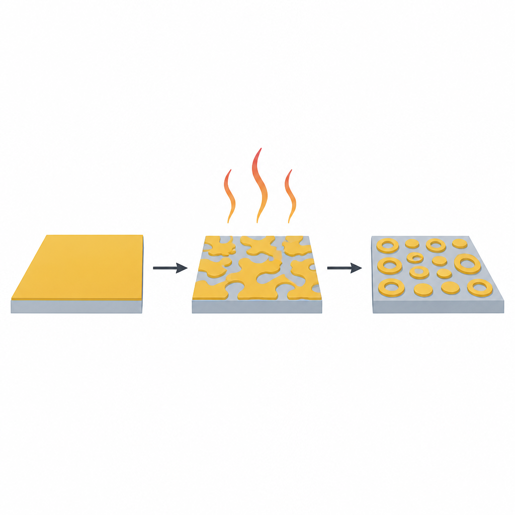
When a very thin solid film on a surface is heated, it can behave a bit like a drying puddle. Holes appear, the edges pull back, and the film eventually breaks into isolated islands. This solid‑state “dewetting” has long been seen as a curiosity, but it also offers a route to create regular patterns without complicated lithography. The challenge has been that the patterns are hard to predict and have usually required expensive, single‑crystal oxide wafers as the underlying surface.
Moving Single‑Crystal Metal onto Ordinary Glass‑Like Surfaces
The team began by growing high‑quality single‑crystal palladium films on silicon, using a copper layer that could later be etched away. Once the copper was dissolved, the palladium floated free and could be placed onto oxidized silicon, a common glass‑like surface used in electronics. Microscopy and diffraction measurements confirmed that, even after transfer, the films largely kept their orderly crystal structure. When these transferred films were patterned into squares with circular holes and then heated, they broke up into strikingly regular rings and islands whose shapes depended on how the patterns were aligned with the crystal directions.
Gas Atmosphere as a Steering Wheel
By changing the mix of argon and hydrogen gases during heating, the researchers could switch which crystal directions were favored as the film broke apart. In some gas conditions, both major in‑plane directions produced stable square‑like rings; in others, only one direction did. Detailed surface measurements showed that tiny amounts of oxygen and hydrogen from the ambient gas were binding to the palladium surface and altering which crystal faces were most “comfortable” to expose. This, in turn, controlled how quickly certain edges retracted and which hole shapes were stable, much like changing friction along different lanes of a racetrack.
Computer Models that Match the Real Patterns
To make the process predictable rather than trial and error, the authors combined three levels of computer modeling. Quantum‑level calculations estimated how strongly gases stick to different crystal faces. Atom‑by‑atom simulations turned these energies into surface tensions and adhesion strengths. Finally, a kinetic Monte Carlo model used those values to simulate how the film’s surface atoms hop and rearrange during heating. With only a few fitted parameters, the simulations reproduced the experimental ring shapes, line stability, and even quantitative dimensions to within about ten percent, confirming that the key physics had been captured.
From Self‑Organized Patterns to Working Devices
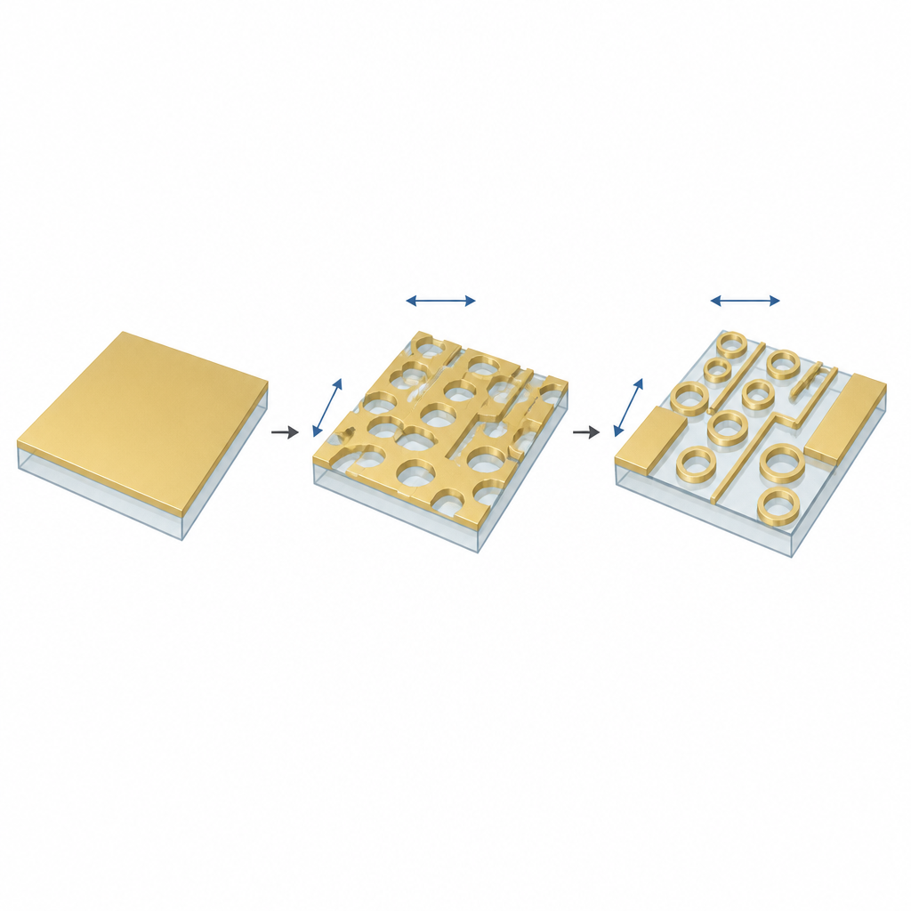
Armed with this understanding, the team designed starting shapes that would dewet into very narrow metal lines separating future transistor regions. After dewetting, they coated the sample with gold, then chemically removed the palladium “mold,” leaving behind finely spaced gold electrodes with submicron gaps between them. Adding a thin layer of an oxide semiconductor across these electrodes produced a simple thin‑film transistor that showed clear switching behavior, demonstrating that the self‑organized patterns can act as real device components.
What This Means for Future Electronics
This work shows that the seemingly messy process of a thin film breaking apart can be tamed and used as a design tool. By transferring single‑crystal metal films onto common substrates and carefully choosing gas conditions and pattern orientation, engineers can predict and program how the film will reshape itself into useful rings and lines. The result is a flexible, materials‑aware way to form tiny, regular structures for electronics and other technologies without relying solely on ever more demanding traditional lithography.
Citation: Ju, S., Lee, S., Kim, D. et al. Predictive patterning via solid-state dewetting of transferred single-crystal films. Nat Commun 17, 4542 (2026). https://doi.org/10.1038/s41467-026-70836-y
Keywords: solid-state dewetting, palladium thin films, nanopatterning, surface energy anisotropy, thin-film transistors