Clear Sky Science · en
Electrostatically tunable moiré-mediated Wigner states via interfacial potential engineering in 2D van der Waals heterostructures
Why tiny patterns in flat materials matter
Today’s quest for better quantum technologies often comes down to how precisely we can trap and move single electrons. This study shows a new way to sculpt the energy landscape inside ultra-thin materials so that electrons not only sit still, but also organize themselves into orderly patterns. By cleverly stacking and twisting atomically thin layers, the authors create tiny repeating "neighborhoods" where electrons behave like artificial atoms, opening paths toward more stable quantum bits and advanced low-power electronics.
Building a layered playground for electrons
The researchers start with a special stacked structure made of two key ingredients: a twisted double layer of the semiconductor molybdenum disulfide (MoS₂) and a very thin film of the semimetal bismuth underneath it, all resting on a supporting base. When the two MoS₂ layers are rotated slightly with respect to each other, their atomic grids interfere to create a large, gentle pattern called a moiré superlattice. This pattern forms a regular array of low-energy spots—like dimples in a mattress—where electrons naturally prefer to sit. At the same time, making the bismuth layer only a few dozen nanometers thick forces its own electrons into discrete standing-wave-like states confined between its top and bottom surfaces.
How two kinds of confinement work together
What makes this platform special is that electrons at the MoS₂–bismuth interface feel both the sideways moiré dimples and the vertical confinement from the thin bismuth film. The team uses low-temperature scanning tunneling microscopy and spectroscopy, tools that can map where electrons live and at what energies. They find that the twisted MoS₂ layer forms well-defined energy bands with very heavy, slow-moving electrons that are easily trapped at the moiré sites. Because the bismuth film naturally donates electrons to the MoS₂, the system is filled without needing external gates, simplifying the design. Within the energy gap of MoS₂, signals mainly come from the bismuth’s quantized states, which become the backbone for the new interface behavior.
Electrons arranging themselves into orderly patterns
By gently changing the probe voltage, the scientists watch how charges appear and disappear at specific moiré sites, forming expanding and shrinking rings and stripe-like patterns in their images. These patterns are signatures of electrons being added to or removed from localized states. The data reveal multiple, regularly spaced energy levels associated with electrons trapped at the interface, consistent with bismuth’s quantum well states. Even more intriguingly, the spatial layout of the trapped electrons differs from place to place: in some regions, three electrons cluster closer to the center of a moiré site in a compact, molecule-like configuration; in others, three electrons spread out into a broader triangular pattern resembling arrangements predicted for so-called Wigner crystals, where repulsion forces electrons into ordered lattices. 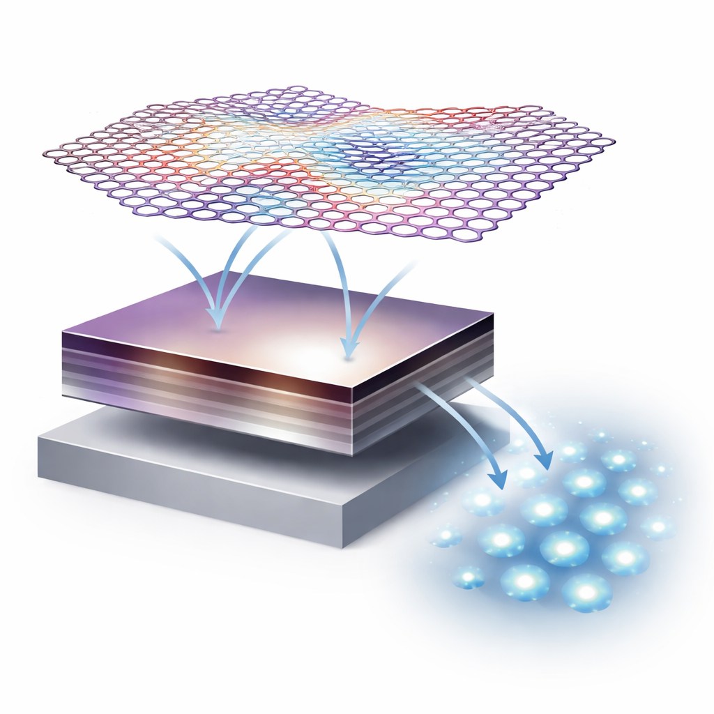
Tuning patterns by changing film thickness
The study shows that the way electrons arrange themselves is not fixed. When the bismuth film is thinner, the spacing between its quantized energy levels is larger and the electrons at the interface behave less tightly localized, favoring more compact electron groupings at the moiré minima. As the bismuth becomes thicker, its confined states move closer together in energy and develop heavier, more localized character. This pushes electrons within each moiré cell to sit farther apart from each other and from the center, enhancing Wigner-like patterns. In effect, the researchers create a “potential-integrated” design: the in-plane moiré pattern and the out-of-plane bismuth confinement jointly determine how many electrons sit in each site, how strongly they interact, and how they arrange themselves in space. 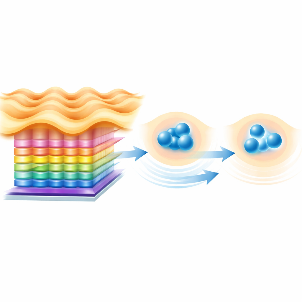
From fundamental order to future quantum bits
For non-specialists, the key message is that the team has demonstrated a controlled way to make electrons self-organize into tiny, repeatable patterns using only carefully chosen materials and thicknesses—no complex wiring or heavy external fields required. These moiré “artificial atoms” can be tuned in three ways at once: by their charge configuration (how electrons are arranged), by their spacing (set by the moiré period), and by their energy levels (set by the bismuth thickness). Such versatility makes this layered platform a promising candidate for building solid-state qubits based on charge, as well as for exploring other exotic phases of matter that arise when electrons are strongly confined and strongly interacting.
Citation: Chen, HY., Hsu, HC., Lin, LS. et al. Electrostatically tunable moiré-mediated Wigner states via interfacial potential engineering in 2D van der Waals heterostructures. Nat Commun 17, 3924 (2026). https://doi.org/10.1038/s41467-026-70614-w
Keywords: moiré superlattice, Wigner crystal, quantum confinement, van der Waals heterostructure, bismuth nanofilm