Clear Sky Science · en
Passivating pinholes for large-area and high-efficiency silicon solar cells with tunnel oxide passivated contact
Why Tiny Flaws Matter for Solar Power
Modern silicon solar panels are already remarkably good at turning sunlight into electricity, but pushing them even closer to their physical limits requires understanding what happens at unimaginably small scales. This study looks deep inside one of today’s leading solar cell designs, called TOPCon, and discovers that what were thought to be harmful flaws at the atomic level can, in fact, be turned into helpful features. By learning how to control these nanoscale “pinholes,” the authors show how to build large, factory-ready solar cells with record-setting efficiency.
A New Kind of Silicon Solar Cell
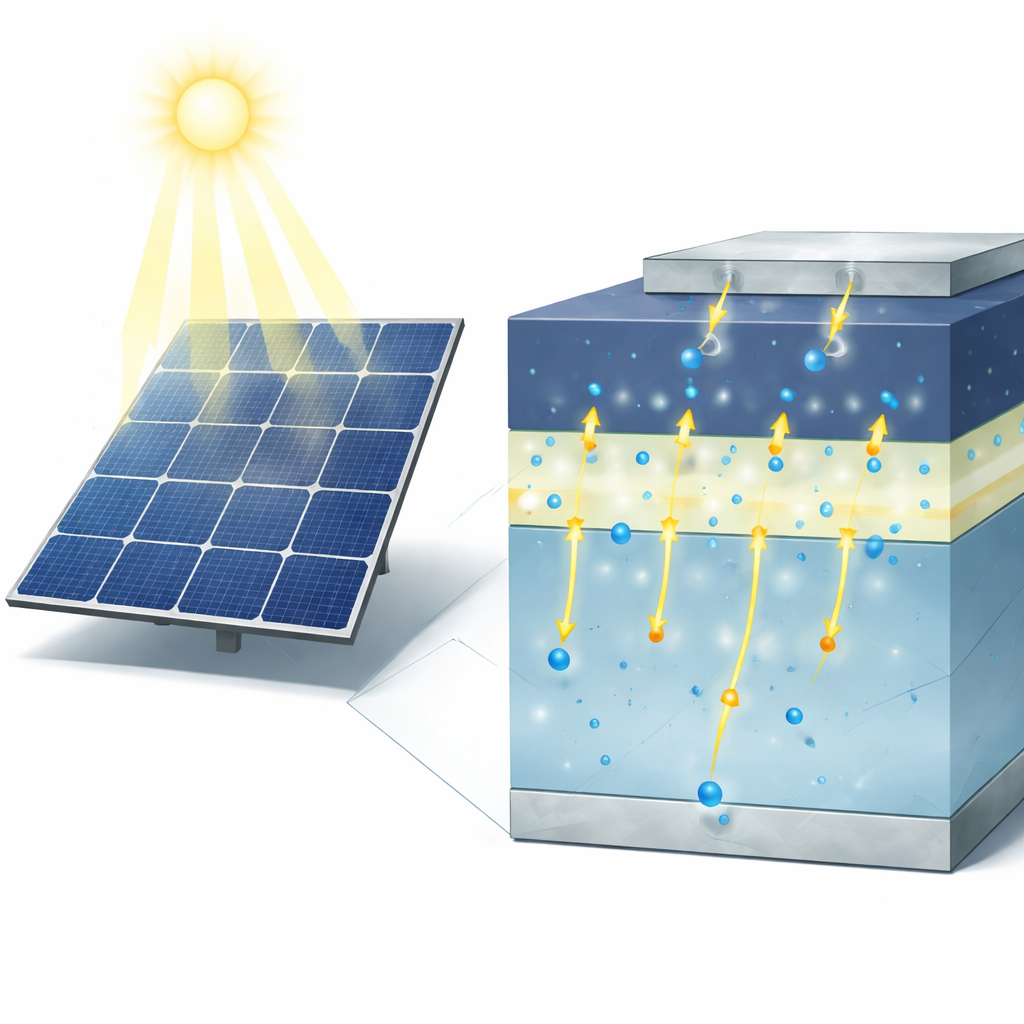
Silicon solar panels now power everything from rooftops to giant desert power plants, and TOPCon (tunnel oxide passivated contact) cells are emerging as a workhorse technology. In these devices, a thin insulating layer of silicon oxide is sandwiched between the main silicon wafer and a heavily doped silicon layer that helps draw out electrical charges. This architecture can, in theory, deliver very high power conversion efficiencies at low cost, making it attractive for the massive build-out of solar needed to reach climate and carbon-neutrality goals. Companies and research institutes have already reported TOPCon cells with efficiencies above 26%, and industrial power prices in some regions have dropped to just fractions of a cent per kilowatt-hour.
The Mystery of Microscopic Gaps
Despite these successes, the microscopic details of how TOPCon cells work have remained murky. In particular, researchers have long debated the role of “pinholes” — tiny spots where the oxide layer is disrupted and the two silicon regions can interact more directly. Conventional wisdom held that these pinholes were mostly bad: areas where the protective oxide was missing, creating defects that let charge carriers recombine and waste energy. Yet experiments and computer models did not fully agree on how harmful pinholes really were, or how many could be tolerated before performance fell off. This uncertainty limited the ability of manufacturers to fine-tune their processes.
Seeing the Interface Atom by Atom
To resolve this puzzle, the team used state-of-the-art electron microscopes capable of imaging individual atomic columns at the interface between the silicon wafer, the oxide, and the polycrystalline silicon layer. They compared industrial-scale TOPCon cells that differed in efficiency by about 1.3 percentage points but looked nearly identical under more conventional microscopes. With higher resolution and chemical mapping, they discovered that not all pinholes are created equal. Some pinholes lack oxygen entirely and create direct silicon–silicon contact riddled with defects; these behave as true “recombinational pinholes” that hurt device performance. Others, however, still contain enough oxygen atoms to chemically “soothe” dangling bonds, while remaining thin enough to let charges tunnel through. The authors term these newly recognized features “passivating pinholes.”
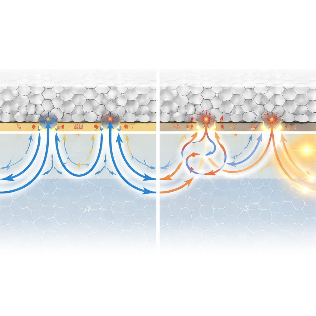
Turning Flaws into Features
By carefully slicing cells along different directions and counting these tiny structures, the researchers found that high-performing devices actually contain an enormous number of pinholes—on the order of a trillion per square centimeter—much more than earlier estimates. Crucially, the best cells are dominated by the passivating type. Modeling shows that what matters most is not the exact size or spacing of pinholes, but how well their surfaces are chemically tamed. If the pinholes are well passivated, they provide many tiny electrical pathways with low resistance, improving the flow of charges without introducing excessive losses. Process measurements support this view: cells rich in passivating pinholes show longer carrier lifetimes, higher open-circuit voltages, lower contact resistance, and uniform performance across large industrial wafers. Using this approach, the team demonstrates commercial-size cells with a certified efficiency of 25.40% and excellent voltage output.
Guiding the Next Generation of Solar Cells
The work suggests a shift in how solar technologists should think about imperfections at interfaces. Instead of striving to eliminate pinholes entirely, the goal becomes to engineer them so that they remain oxygen-rich and electrically gentle. The study lays out practical levers—such as oxidation temperature, oxygen supply, and subsequent heat treatments—that manufacturers can tune to favor passivating pinholes over harmful ones. For a layperson, the key message is that by mastering control over structures only a couple of billionths of a meter across, engineers can squeeze more electricity from the same sunlight, lowering costs and accelerating the spread of clean energy technologies.
Citation: Zhang, W., Zhang, K., Bai, Y. et al. Passivating pinholes for large-area and high-efficiency silicon solar cells with tunnel oxide passivated contact. Nat Commun 17, 2490 (2026). https://doi.org/10.1038/s41467-026-70511-2
Keywords: silicon solar cells, TOPCon, pinholes, interface passivation, photovoltaic efficiency