Clear Sky Science · en
High-speed Si-Ge avalanche photodiode with a gain-bandwidth product of 7564 GHz
Why Faster Light Sensors Matter
Every photo, video call, and AI query you send races through vast networks of glass fibers as tiny flashes of light. At the end of each fiber, a light sensor must convert those flashes into electrical signals the chips can understand. As data centers and cloud computing push toward ever higher speeds, today’s light sensors are becoming a bottleneck. This paper reports a new silicon–germanium avalanche photodiode—a highly sensitive light detector—that breaks speed records while remaining compatible with standard chip-making technology, pointing the way toward faster and more energy‑efficient internet and computing hardware.
Turning Faint Light into Strong Signals
Avalanche photodiodes are special light sensors that don’t just detect light—they also amplify the resulting electrical signal inside the device itself. That built‑in gain lets receivers work with very weak light, which is crucial for long fiber links and for reducing the power used per bit of data. The authors focus on a key performance yardstick called the gain‑bandwidth product, which combines how much amplification you get with how quickly the device can respond. Pushing this number higher means you can detect extremely fast data streams without drowning in noise. Traditional materials used in telecom light detectors, like certain compound semiconductors or pure germanium, either generate too much noise or are hard to integrate densely on silicon chips. This work instead exploits a carefully engineered combination of silicon and germanium to get the best of both worlds.

Splitting the Work Between Two Materials
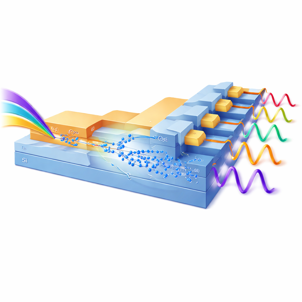
The new device uses a layout called a lateral separate‑absorption‑charge‑multiplication structure. In simple terms, the silicon and germanium layers each get a specific job. Germanium, which absorbs light efficiently at the wavelengths used in data communications, serves as the light‑catching region. Silicon, which supports quieter electron multiplication, serves as the built‑in amplifier. The team shapes the internal electric field so that it is strong where they want electrons to avalanche in silicon, but kept much weaker in the germanium. This careful "field engineering" greatly cuts unwanted leakage currents and noise, while still sweeping the photo‑generated carriers quickly enough to keep the device fast. They also avoid direct metal contacts on top of the germanium, which reduces defects and further suppresses dark current.
Recycling Light to Boost Efficiency
Beyond the internal amplifier, the researchers tackle another challenge: how to collect as much of the incoming light as possible without slowing the device down. Simply making the germanium region larger would improve light absorption, but it would also make carriers take longer to cross, limiting speed. Instead, the team adds a tapered input waveguide that gently funnels light into the tiny active region, and a distributed Bragg reflector at the back end that acts like a microscopic mirror. Light that slips through the germanium on the first pass is reflected back for a second chance to be absorbed. Simulations and measurements show that this strategy tightens the light confinement in the germanium layer and improves responsivity by about one‑third, all while keeping the structure compact and fast.
Beating Records at Terabit Data Rates
To judge real‑world performance, the team measures how the device responds to high‑speed optical signals. They find that at modest light levels and a reverse voltage of 12.5 volts, the photodiode can amplify the signal more than two hundredfold while maintaining an electrical bandwidth of around 31 gigahertz. Under low‑power illumination, this combination yields a record gain‑bandwidth product of 7564 gigahertz, far beyond previous silicon–germanium designs. Eye‑diagram and bit‑error tests—standard tools in communications engineering—show that the device can directly receive 100‑gigabit‑per‑second traditional signals and 200‑gigabit‑per‑second multilevel signals with sensitivities compatible with practical error‑correction schemes, even without adding a separate electronic amplifier. They also build an eight‑channel array tuned to slightly different wavelengths, demonstrating clean 200‑gigabit‑per‑second operation on each channel for wavelength‑division multiplexed links.
What This Means for Future Networks
From a layperson’s perspective, the key takeaway is that the authors have built a tiny light sensor that can see very weak signals while keeping up with extremely rapid data streams, and they have done so using technology that fits into the existing silicon chip ecosystem. By carefully assigning light‑absorption and amplification roles to germanium and silicon, shaping the electric field to minimize noise, and recycling light with a miniature mirror, they achieve unprecedented performance in a compact device. Such high‑speed, low‑noise photodiodes could help future data centers move more information through each fiber, reduce power consumption per bit, and support emerging applications such as quantum communication and advanced LiDAR, all while leveraging the manufacturing infrastructure already used for modern microelectronics.
Citation: Xue, J., Cheng, C., Bao, S. et al. High-speed Si-Ge avalanche photodiode with a gain-bandwidth product of 7564 GHz. Nat Commun 17, 3730 (2026). https://doi.org/10.1038/s41467-026-70461-9
Keywords: avalanche photodiode, silicon photonics, optical communication, high-speed detectors, wavelength-division multiplexing