Clear Sky Science · en
Atomic imaging for hydrogen and boron aggregates in boron-doped diamond by spectro-photoelectron holography
Why tiny atoms in diamond matter
Diamonds are famous for their sparkle, but scientists prize them for something less glamorous: their ability to conduct electricity in unusual ways when a few foreign atoms are added. This study looks deep inside boron‑doped diamond, a material that can even become superconducting at low temperatures, and asks a surprisingly basic question: exactly where do the boron and hydrogen atoms sit in the crystal, and how does that change the diamond’s behavior? By turning electron waves into a kind of atomic‑scale hologram, the researchers directly map these hidden arrangements for the first time.
How adding guests changes a crystal home
In many modern technologies, from computer chips to power electronics, engineers “dope” crystals with tiny amounts of impurity atoms to tune their properties. In diamond, substituting a few carbon atoms with boron turns the crystal into a p‑type semiconductor by creating mobile positive charges, or holes. But when more and more boron is added, a puzzling problem appears: a growing fraction of these boron atoms stop contributing to electrical conduction. Earlier work suggested that boron atoms might clump together or be neutralized by hydrogen, but direct proof of their exact positions inside the diamond lattice was missing.
A new way to see atoms with electron waves
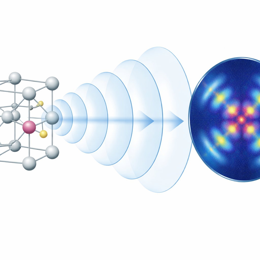
The team used a technique called spectro‑photoelectron holography, which turns electron emission into a three‑dimensional map of nearby atoms. When X‑rays hit the sample, they knock electrons out of specific atoms. Some of these electrons travel straight to a detector, while others bounce off neighboring atoms before arriving. The overlapping waves form an interference pattern—a hologram—that encodes the arrangement of atoms around the emitting site. By measuring these patterns for selected electronic “flavors” of boron and comparing them with detailed computer simulations, the researchers could distinguish different local environments: isolated boron atoms, boron pairs, and boron linked with hydrogen.
Finding boron pairs and hidden hydrogen
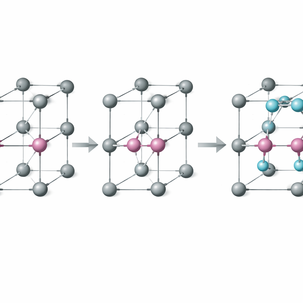
First, the authors confirmed that one component of the boron signal comes from single boron atoms that simply replace carbon atoms in the diamond lattice. Their hologram closely matched that of ordinary carbon, showing that these boron atoms sit at well‑ordered, electrically active sites. A second component, however, produced a slightly blurred pattern. By systematically testing candidate structures, the team found that the best match corresponded to boron dimers—neighboring boron atoms bonded next to each other. In this case, the bond between the two boron atoms is stretched compared to a normal carbon–carbon bond, subtly distorting the surrounding lattice and broadening the hologram.
How hydrogen sneaks in and switches boron off
Two other boron signals carried the fingerprint of nearby hydrogen. To highlight these subtle differences, the researchers divided their holograms by the pattern from isolated boron, producing “ratio images” that reveal extra scattering from additional atoms. Bright regions along different crystal directions pointed to hydrogen trapped at two distinct positions relative to boron: a bridging site, where hydrogen sits between boron and a neighboring atom, and an anti‑bonding site, where hydrogen lies just beyond the boron–carbon bond. Simulations using simple clusters of boron, carbon, and hydrogen reproduced these bright spots, confirming the presence of specific boron–hydrogen complexes. The spectral shifts show that, in these complexes, boron becomes more positively charged while hydrogen behaves like a tiny proton, effectively neutralizing the boron’s ability to donate charge carriers.
What this means for future diamond devices
By tying subtle shifts in the boron spectra to concrete atomic pictures, this work shows that both boron clustering and boron–hydrogen complexes are responsible for “turning off” many boron atoms in heavily doped diamond. Hydrogen introduced during film growth or surface treatments does not merely decorate the surface—it can become lodged in precise lattice sites that trap and passivate boron. Beyond resolving a long‑standing puzzle in boron‑doped diamond, the study demonstrates that spectro‑photoelectron holography is a powerful new tool for directly imaging hydrogen and other light atoms around dopants, offering a way to rationally design cleaner, more efficient electronic and quantum devices based on diamond and other advanced materials.
Citation: Tomita, H., Hosoda, W., Taniguchi, T. et al. Atomic imaging for hydrogen and boron aggregates in boron-doped diamond by spectro-photoelectron holography. Nat Commun 17, 3482 (2026). https://doi.org/10.1038/s41467-026-70231-7
Keywords: boron-doped diamond, hydrogen defects, photoelectron holography, dopant passivation, superconducting semiconductors