Clear Sky Science · en
Defect-evolved quadrupole higher-order topological nanolasers
Light Trapped in a Tiny Corner
Lasers are everywhere, from high‑speed internet cables to phone sensors, but making them ever smaller and more efficient is a constant challenge. This research shows how ideas from the strange world of “topological” physics can be used to trap light in an ultra‑tiny corner of a nanostructure and turn that trapped light into a remarkably stable, low‑power laser operating in the same wavelength range used for fiber‑optic communications.
Guiding Light with Hidden Order
Over the past decade, scientists have learned to control light using concepts borrowed from topological insulators—materials whose internal patterns give rise to robust conducting channels along their edges. In photonic crystals, carefully arranged patterns of holes or pillars can play a similar role for light, creating edge pathways that are unusually resistant to defects. Recently, a new class of systems called higher‑order topological insulators promised something even more striking: not just protected edges, but tiny, well‑defined “corner” spots where light can be tightly confined in three dimensions, ideal for miniature lasers.
Turning Tiny Defects into a New Kind of Order
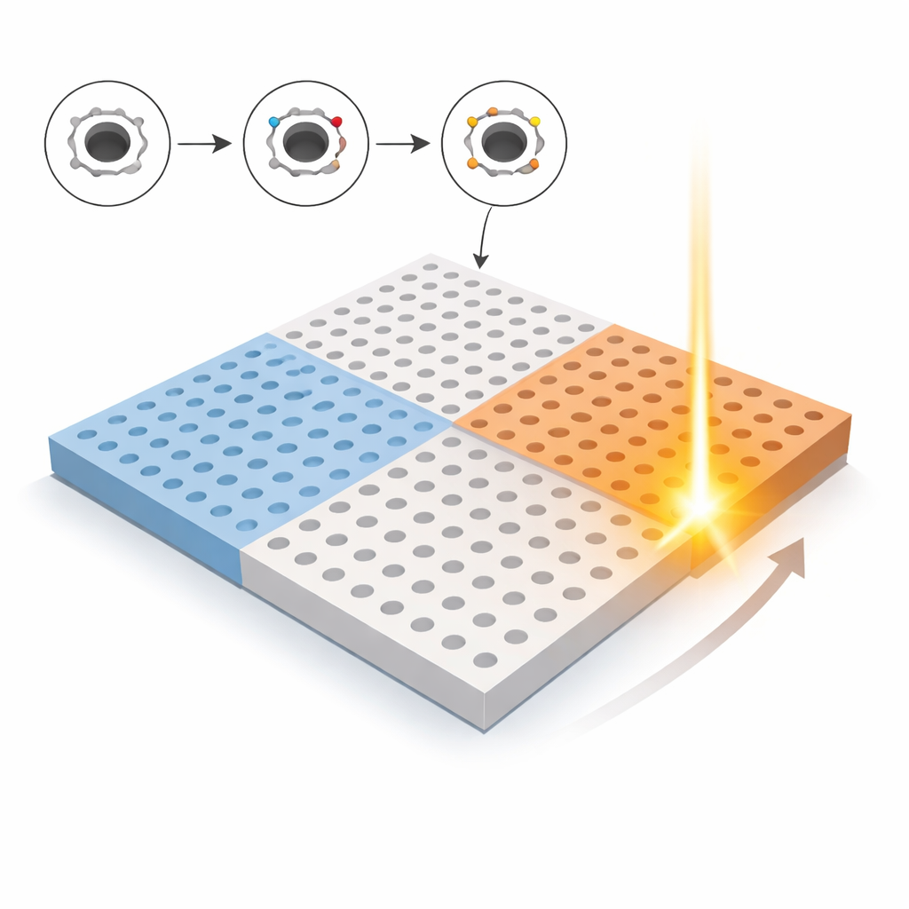
Traditional designs for these corner‑state lasers often rely on changing the spacing between unit cells in a repeating pattern. In this work, the authors take a different path: they sculpt small geometric “defects” into each air hole of a square photonic crystal and then systematically change those defects in opposite directions. By rotating the notch‑like defects clockwise in one region and anticlockwise in another, they create two domains that are topologically distinct even though they share the same basic lattice. Where these two domains meet at a single corner, the mathematical description of the structure predicts a special, highly localized light mode that behaves like a topological quadrupole “corner state.”
A Corner That Becomes a Laser
To turn this corner state into a working device, the team fabricates the pattern in a semiconductor slab containing InGaAsP multiple quantum wells, which act as the gain medium that amplifies light. Numerical simulations show that the corner state lies in a clean frequency window between bulk modes, with a very small mode volume and high quality factor, meaning the light is tightly confined and leaks out only weakly. Experiments confirm that when the structure is pumped with a pulsed red laser, a sharp emission line appears at about 1.56 micrometers in the telecom C‑band. The output follows the hallmark signatures of lasing: a clear threshold in the light‑versus‑input curve, rapid narrowing of the emission line, and a near‑field pattern concentrated at the corner with only weak extension along the edges.
Stable Performance and Tunable Color
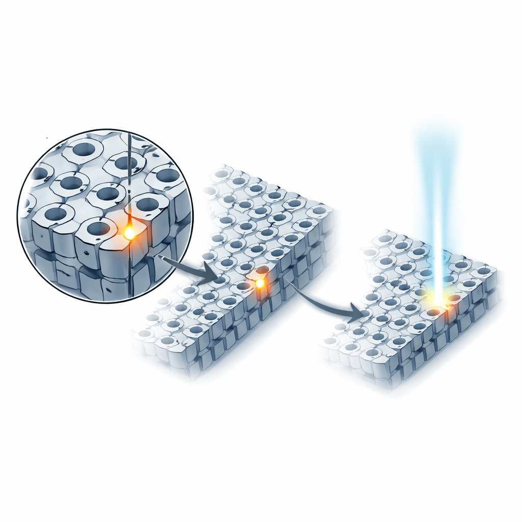
Beyond simply proving that the corner state can lase, the device shows practical strengths. It operates in a single spatial mode over a wide range of pump powers and remains stable up to 70 °C, an important consideration for real‑world integration. The measured threshold is extremely low—about half a microwatt of average pump power—thanks to the tight confinement and reduced radiation loss of the topological corner. A particularly appealing feature is that the emission wavelength can be tuned simply by adjusting how much the tiny defects evolve. As the notch sizes are changed, the resonance of the corner state shifts smoothly, allowing the laser color to be moved across roughly 24 nanometers without altering the overall footprint or basic design.
Why This Matters for Future Photonics
In essence, this work shows that cleverly engineered nanoscale defects can drive a special kind of topological phase that funnels light into a single corner and turns it into a robust, energy‑efficient laser. For non‑specialists, the takeaway is that “hidden order” in a patterned semiconductor can protect and shape light in ways that ordinary designs cannot, enabling tiny lasers that are both tunable and resilient to imperfections. Such defect‑evolved quadrupole nanolasers could become key building blocks for dense optical chips used in communications, sensing, and even quantum technologies, where reliable, compact sources of coherent light are essential.
Citation: Guo, S., Huang, W., Tian, F. et al. Defect-evolved quadrupole higher-order topological nanolasers. Nat Commun 17, 3238 (2026). https://doi.org/10.1038/s41467-026-70056-4
Keywords: topological photonics, nanolasers, photonic crystals, telecom-band light, on-chip optics