Clear Sky Science · en
MXene-driven nanoscale field-effect junction for advanced 4-terminal perovskite/silicon tandem solar panels
Turning Sunlight into More Power
Solar panels are now common on rooftops and in fields, yet even our best commercial panels waste a large share of the Sun’s energy. This study shows a practical way to squeeze more electricity from the same sunlight by stacking two different solar technologies—an advanced material called perovskite on top of silicon—and making them work together efficiently in real, outdoor conditions. The work focuses not just on breaking lab records, but on building large, durable panels that could fit smoothly into today’s solar factories.
Why Two Solar Layers Are Better Than One
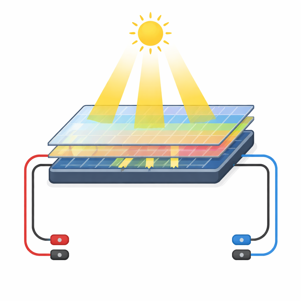
Silicon solar cells dominate the market and are approaching their theoretical efficiency limit of about 30%. Perovskite solar cells, a newer class of materials, have raced ahead in efficiency in the lab, but face challenges when scaled to large, stable modules. By stacking a semi-transparent perovskite layer on top of a silicon cell, each layer can harvest different colors of sunlight: the perovskite uses the higher-energy part of the spectrum and lets the rest pass through to the silicon. In a four-terminal configuration, the two layers operate like separate mini-power plants that share the same sunlight but keep their electrical circuits independent, simplifying integration with existing silicon production lines.
Building a Smarter Perovskite Layer
The key innovation of this work is how the authors re-engineer the perovskite itself to move charges more cleanly. They introduce two ingredients into the perovskite structure. First, a class of ultra-thin materials known as MXenes, carrying chlorine atoms, is mixed into the perovskite precursor. These MXene flakes collect near the buried interface and help create a region that behaves more like an electron-rich side. Second, a special organic additive is applied near the surface to gently change the material there into a hole-rich side and to heal defects that would otherwise waste energy as heat. Together, these two treatments form what the authors call a “field-effect junction” inside a single perovskite layer—mimicking the beneficial internal electric field of a traditional p–n junction without needing to stack two separate perovskite films.
From Tiny Cells to Real Panels
In small test cells, this engineered perovskite design delivers higher voltage, more current, and less performance hysteresis, all signs of fewer defects and more efficient charge collection. The team then scales the approach up. They fabricate semi-transparent perovskite modules with an active area of 60 square centimeters, using greener processing solvents and laser patterning to interconnect 24 small cells on a single glass sheet. These modules reach efficiencies above 16%, a strong result for devices that must both generate power and transmit enough light to the silicon layer beneath. Importantly, the efficiency loss when moving from tiny lab cells to these larger modules is kept relatively small, which is vital for industrial adoption.
Putting Tandem Panels to the Test
Next, the perovskite modules are laminated on top of commercial bifacial silicon heterojunction cells, creating four-terminal tandem panels around 0.2 square meters in size. One demonstrator reaches a power conversion efficiency of about 21% under standard indoor test conditions. A larger panel, combining 16 perovskite modules with four bifacial silicon cells, delivers nearly 19.5% efficiency in an outdoor test and can exceed 23 milliwatts per square centimeter when it also collects light reflected from the ground. Installed in Crete and monitored for three months, the perovskite top panel keeps more than 95% of its initial power, with only a slow, modest decline mainly in the fill factor, while the silicon part shows no obvious degradation.

What This Means for Future Solar Power
For a non-specialist, the bottom line is that the researchers have shown a realistic path to more powerful solar panels without overhauling the silicon infrastructure that already exists. By using MXenes and surface treatments to shape an internal electric field inside the perovskite, they boost efficiency, stability, and scalability all at once. The resulting four-terminal perovskite/silicon tandems are efficient, can be produced on areas comparable to real panels, and survive months of outdoor operation. With further work to cut costs and refine manufacturing, this field-effect design could help bring next-generation tandem solar panels from the lab onto rooftops and solar farms worldwide.
Citation: Agresti, A., Pescetelli, S., Viskadouros, G. et al. MXene-driven nanoscale field-effect junction for advanced 4-terminal perovskite/silicon tandem solar panels. Nat Commun 17, 3394 (2026). https://doi.org/10.1038/s41467-026-70002-4
Keywords: perovskite silicon tandem, MXene, field effect junction, semi transparent solar modules, bifacial silicon