Clear Sky Science · en
Oriented ion migration in dielectric Sb4O5Cl2 single crystals for multifunctional two-dimensional electronics
Smart Switches for Tiny Electronics
Electronic gadgets are shrinking to the scale of a few atoms, but the insulating layers that control them have not kept up. This study introduces a new crystal, called Sb4O5Cl2, that behaves like a smart insulator: it not only turns 2D transistors on and off efficiently, but can also gently rearrange charged atoms inside itself to reprogram how a neighboring circuit behaves. That combination could help build faster, more versatile chips and brain‑like hardware for future artificial intelligence.
A New Kind of Crystal Building Block
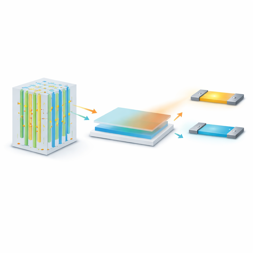
The researchers first grew large, plate‑like single crystals of Sb4O5Cl2 using a vapor process, then peeled them down to very thin sheets. Inside each sheet, positively and negatively charged layers repeat in an orderly fashion, leaving regularly spaced channels that host mobile chloride ions. Because the structure is highly ordered rather than glassy or randomly grained, ions have well‑defined paths to move along without damaging the surrounding lattice. Measurements and computer calculations show that the material has a wide energy gap—so it acts as a good electrical insulator—yet still responds strongly to electric fields because of the motion of these ions.
A Powerful, Gentle Gate for 2D Transistors
When used as the insulating gate layer beneath ultrathin molybdenum disulfide (MoS2) transistors, Sb4O5Cl2 provides unusually strong control. The devices can switch their current by more than a billion‑fold while operating at low voltages, leak almost no current through the insulator, and allow charges in the MoS2 to move relatively freely. These advantages stem from the crystal’s large dielectric constant, meaning it can store a lot of electrical influence in a small thickness. At the same time, its layered surface forms a clean, gently interacting contact with the 2D semiconductor, avoiding many of the defects and roughness that plague conventional oxide insulators.
Ion Motion as an Invisible Knob
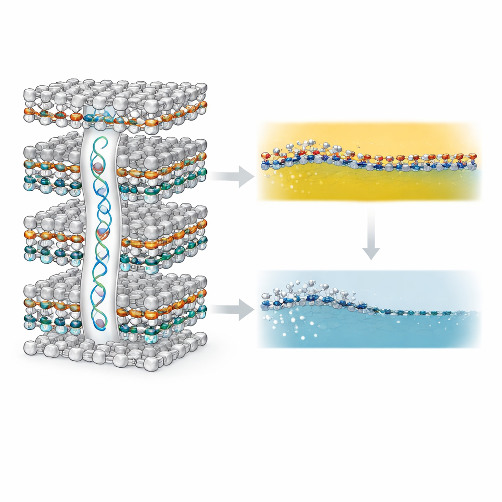
The real novelty appears when the team treats the Sb4O5Cl2 layer not just as a passive insulator, but as an active control element. By applying a voltage across the crystal, they can nudge chloride ions to drift toward or away from the interface with the MoS2. When ions pile up at this boundary, they effectively donate extra negative charge, driving the MoS2 into a highly conductive, metal‑like state. When ions are pulled back, empty sites remain that tend to trap electrons, restoring a less conductive, semiconducting state. This switching happens repeatedly without tearing apart the crystal structure, and the two states remain stable for minutes to nearly an hour even after the voltage is removed, giving the device non‑volatile memory behavior.
Borrowing Tricks from the Brain
Because the conductance of the MoS2 channel can be tuned gradually by ion motion, not just flipped fully on or off, the devices can mimic the way biological synapses strengthen or weaken in response to activity. The authors use sequences of voltage pulses to program many intermediate levels of conductance that persist for hundreds of seconds. They show that this behavior can preprocess noisy images: when connected conceptually to a simple neural‑network model, the ion‑controlled devices help clean up grainy pictures of clothing items before classification. With this built‑in hardware filtering, the recognition system learns faster and reaches higher accuracy than without it.
Why This Matters for Future Tech
In everyday terms, this work demonstrates an insulating crystal that pulls double duty: it acts as a high‑quality gate for tiny transistors and as a reversible, damage‑free dial for their internal state. By steering ions along ordered channels in Sb4O5Cl2, engineers can move a 2D semiconductor smoothly between “good wire” and “good switch” modes and hold it there without constant power. That combination of efficiency, stability, and reprogrammability makes the material a promising building block for compact memory, logic, and neuromorphic circuits that more closely resemble the adaptable processing of a brain.
Citation: Li, Z., Gou, G., Xu, X. et al. Oriented ion migration in dielectric Sb4O5Cl2 single crystals for multifunctional two-dimensional electronics. Nat Commun 17, 2986 (2026). https://doi.org/10.1038/s41467-026-69869-0
Keywords: two-dimensional electronics, ionic dielectric, MoS2 transistor, neuromorphic device, ion migration