Clear Sky Science · en
Micro-LED/van der Waals heterointegration for in-pixel processing display architecture
Smarter Screens at the Edge
Video calls that feel instant, augmented reality that doesn’t make you dizzy, tiny wearables that see and understand the world—these all demand displays that do more than just show pictures. This research describes a new kind of screen pixel that can both compute and shine, promising faster, clearer, and more energy‑efficient visual devices for everything from phones and headsets to smart sensors.
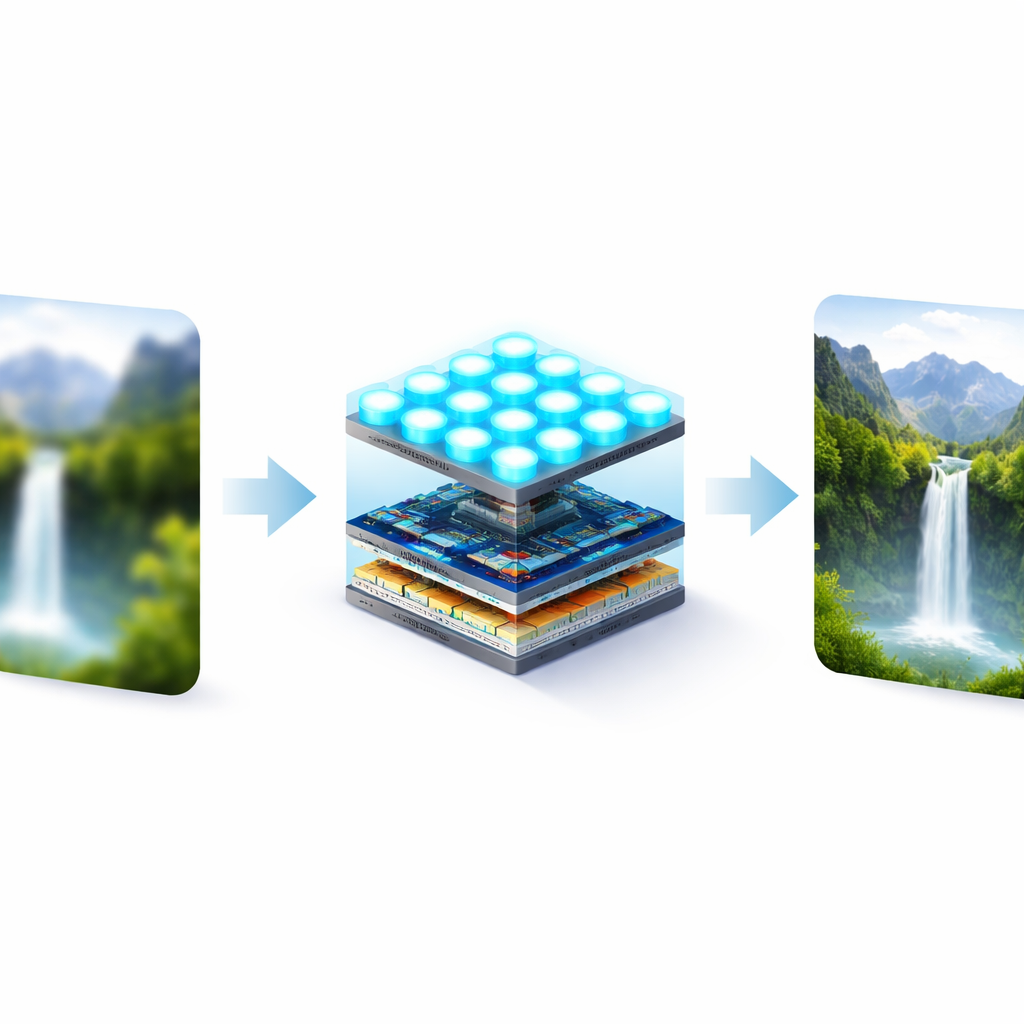
Why Moving Data Is Slowing Us Down
Today’s smart displays rely on a familiar setup: separate chips handle heavy image processing, then send streams of data to the display panel that only turns pixels on and off. As images get larger, frame rates climb, and tasks like denoising, enhancement, and recognition become standard, this constant back‑and‑forth turns into a traffic jam. The result is latency, extra power draw, and sometimes visible lag or blur—problems that grow worse in high‑frame‑rate or high‑dynamic‑range displays used in gaming, virtual reality, and edge AI devices.
Turning Each Pixel into a Tiny Brain
The authors tackle this bottleneck by redesigning what a pixel can do. They build a 16 × 16 array of micro‑LED pixels in which each light‑emitting diode is driven by a special transistor made from an ultra‑thin material called MoS₂. Unlike a conventional switch, this transistor can both remember and process information by storing multiple levels of electrical conductance. Together, the one‑transistor–one‑diode units form a compact “in‑pixel processed micro‑LED” cell: it emits bright, fast, stable light while also behaving like a small analog memory and calculator sitting directly under each point of the image.
How the New Pixel Learns and Adjusts
At the heart of this design is a carefully engineered relationship between the voltage sent to a pixel and the brightness it produces. The device shows three distinct regions: no light at low voltages, a predictable linear zone in the middle, and saturation at high voltages. This “segmented” behavior naturally matches how contrast enhancement works, allowing the system to darken background noise, stretch mid‑tones, and preserve bright highlights simply by choosing the right voltages. At the same time, the MoS₂ transistor can be gently reprogrammed with electrical pulses so that its conductance—and therefore the pixel brightness—changes in many finely spaced steps and then holds that state without continuous power. The researchers show that this synapse‑like behavior enables long‑lasting brightness memory, smooth multilevel tuning, and reliable operation at high speeds up to 5000 times per second.
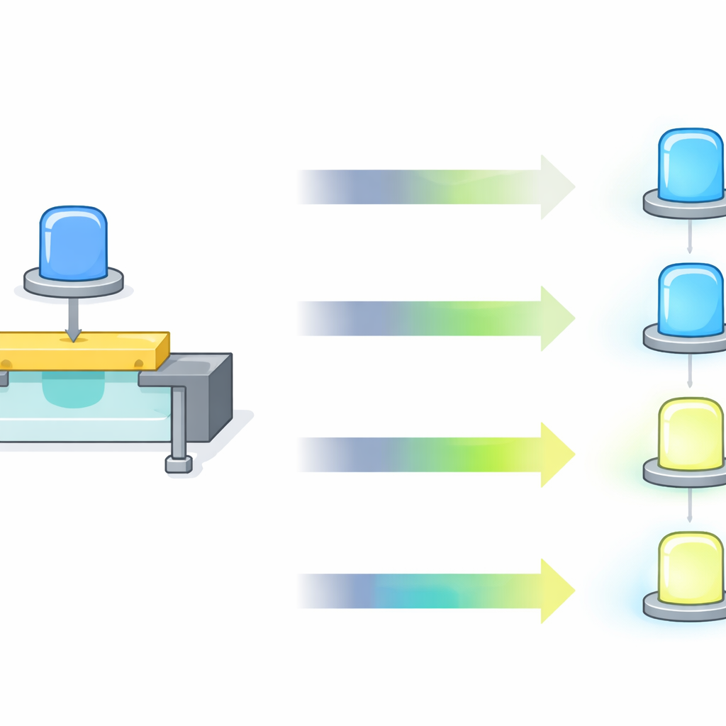
Seeing, Cleaning, and Recognizing Images On the Panel
To prove that computation inside the display is more than a lab curiosity, the team builds a full hardware pipeline around their pixel array. Noisy letter patterns are first converted into voltages that drive the pixels according to the device’s built‑in contrast curve. Without calling on a distant graphics processor, the array itself sharpens the letters by suppressing speckle and boosting real strokes, producing clearer images directly on the panel. Next, the same pixels are used as the core of a simple neural network: trained weights from software are translated into conductance levels in each transistor. When test letters are fed in as voltage patterns, the array performs the multiply‑and‑add operations needed for recognition through its own currents and brightness changes. The in‑panel processing boosts classification accuracy from about 80% for the raw noisy inputs to over 99% after in‑pixel enhancement, with only tiny deviations from the software‑only model.
From Lab Prototype to Everyday Devices
Beyond the initial SiO₂ gate design, the researchers also test versions using a high‑κ dielectric material (HfO₂), which lowers operating voltages and improves energy efficiency while preserving stable memory and light output over many cycles. The pixels are small (20 × 35 micrometers), bright (exceeding 300,000 candelas per square meter), and densely packed, making them compatible with high‑resolution displays. Because processing happens where the light is made, this architecture reduces data movement, trims latency, and creates a tight feedback loop between sensing, computing, and showing. In everyday terms, it points toward future screens that don’t just display what another chip decides, but actively help clean, compress, and understand visual information right at the surface of each glowing dot.
Citation: Wang, F., Wu, Y., Chu, H. et al. Micro-LED/van der Waals heterointegration for in-pixel processing display architecture. Nat Commun 17, 3049 (2026). https://doi.org/10.1038/s41467-026-69786-2
Keywords: micro-LED displays, in-pixel computing, intelligent screens, edge AI hardware, neuromorphic electronics