Clear Sky Science · en
Anapole-state-enhanced 2D chiral photodetector operating in the near-infrared second window
Seeing deeper with gentler light
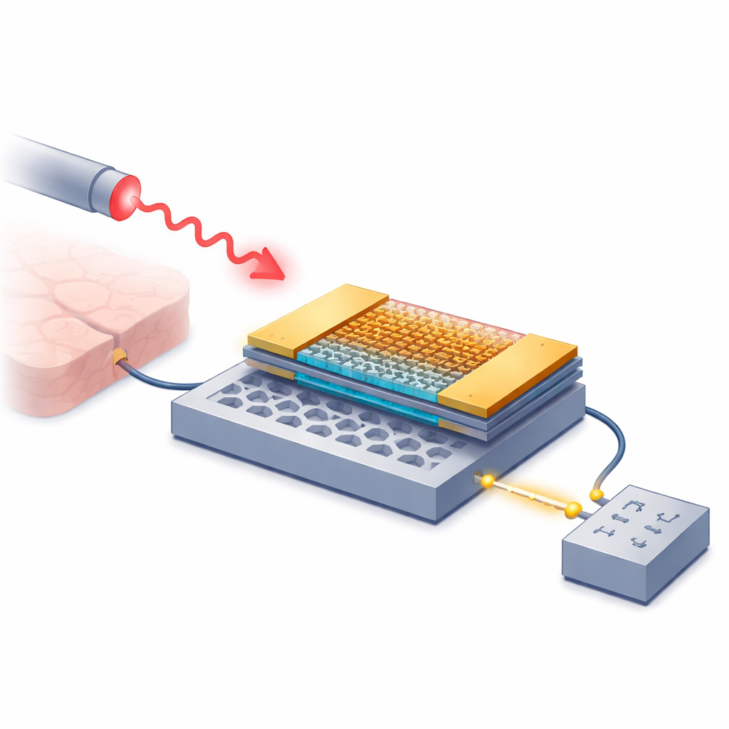
Light detectors are everywhere, from smartphone cameras to medical scanners, but most are bulky and tuned to a narrow slice of the spectrum. This study reports a tiny, ultrathin light sensor that works in the so‑called second near‑infrared window, a range of wavelengths especially useful for peering deep into biological tissue and for carrying data through optical fibers. By sculpting metal at the nanoscale and stacking atom‑thin crystals, the authors massively boost the detector’s sensitivity and even teach it to tell left‑handed from right‑handed swirling light, a key step toward compact, multifunctional optical chips.
Why these faint colors of light matter
The second near‑infrared window, spanning roughly 1000 to 1700 nanometers, is prized because light in this range slips through skin and tissue with relatively little loss and also travels long distances in glass fibers. Conventional semiconductor detectors that work here, such as those based on InGaAs, are effective but rigid, expensive, and hard to shrink to truly microscopic scales. Two‑dimensional materials—crystals just one atom thick—promise a different route. They are flexible, easy to stack into custom structures, and interact strongly with light. Unfortunately, their natural electronic “gaps” usually limit them to visible wavelengths, leaving the medically and technologically important near‑infrared band largely out of reach.
Stacking atom‑thin sheets on a sculpted metal carpet
The team tackles this by marrying a van der Waals heterostructure—two different monolayers of transition metal dichalcogenides, MoS₂ and WSe₂—with a carefully carved silver surface known as a plasmonic metasurface. The 2D stack already hosts a zoo of bound electron–hole pairs called excitons, including hybrid ones that feel both layers at once, slightly extending its sensitivity. The silver below is etched into a regular array of cross‑shaped grooves that trap incoming light into tightly confined patterns. In certain geometric conditions, these grooves support exotic “non‑radiating” field arrangements called anapole states and quasi‑bound states in the continuum. Rather than sending energy back out as scattered light, these states bottle it up in extremely small volumes right where the 2D layers sit.
Turning rare two‑photon events into a strong signal
In the near‑infrared range, each photon is too weak to kick an electron across the material’s gap in one go. Instead, the detector relies on two‑photon absorption: two low‑energy photons arriving nearly at once combine their energy to excite an electron. Under normal circumstances this is a feeble, nonlinear process. Here, the metasurface’s intense local fields make these rare events far more common. The same field concentration also drives oscillations in the silver that shed energetic “hot” charge carriers, which can jump into the 2D layers and contribute to current even when the photon energy is below the gap. Experiments show that, at the key telecom wavelength of 1550 nanometers, the resulting device achieves a responsivity of about 1.35 amperes per watt—roughly fifty thousand times higher than the same 2D stack placed on an ordinary glass‑on‑silicon chip.
Teaching the detector to feel the twist of light
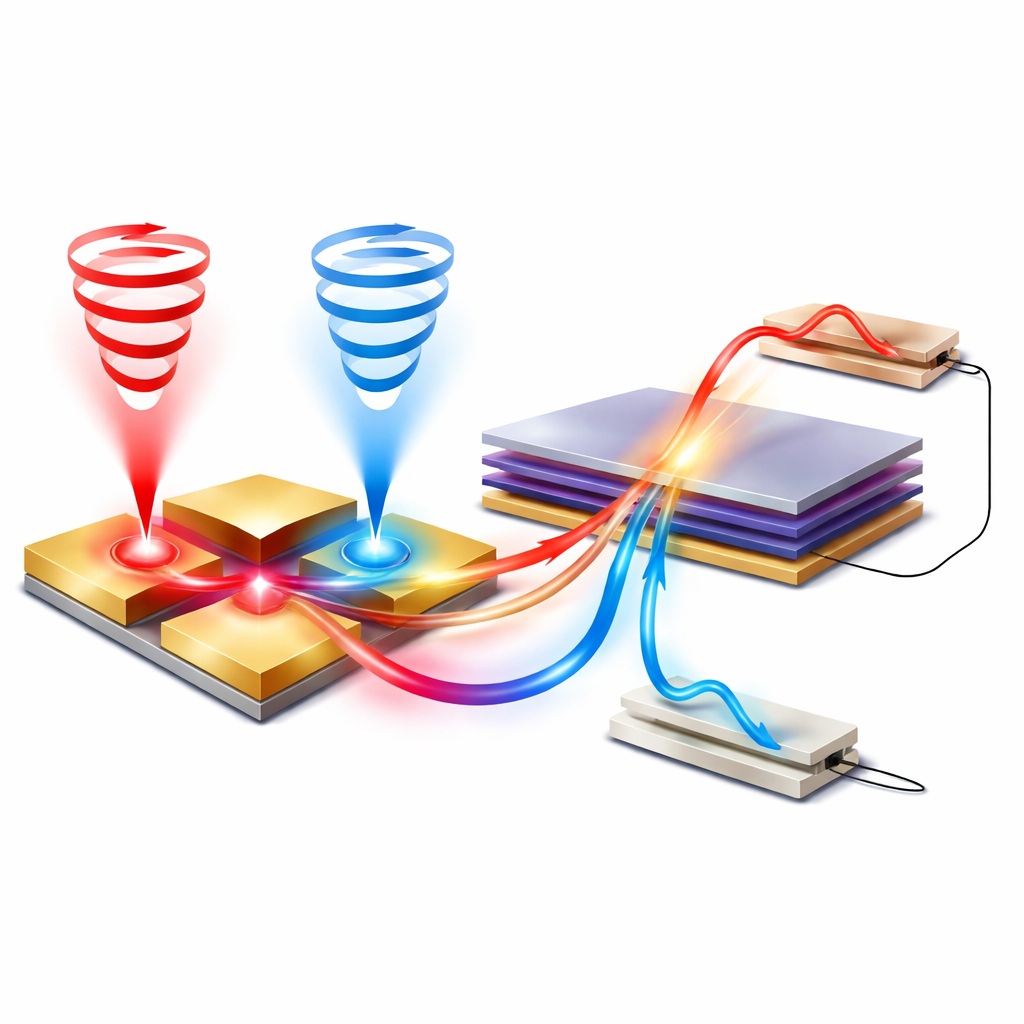
Beyond sheer sensitivity, the authors engineer the metasurface pattern so that it responds differently depending on the polarization of incoming light. By exploiting different resonances for horizontal and vertical orientations, they obtain strong contrast for linearly polarized beams. Then they deliberately break the mirror symmetry of the groove pattern along one direction, making the structure “chiral” in the plane. Under circularly polarized light—where the electric field traces a left‑ or right‑handed spiral—this asymmetry causes one handedness to excite strong field patterns and the other to couple much more weakly. As a result, the same nanostructured area can generate several times more current for one twist of light than for the opposite, with discrimination ratios up to 7.2 around 1550 nanometers.
From lab prototype to future light‑guided gadgets
In simple terms, the researchers have created a paper‑thin light meter that sees in a difficult color band, turns very weak signals into large electrical currents, and can tell how the light is oriented and twisted—all at room temperature. The work shows how extreme control of light on a nanoscale metal surface, combined with stacked atom‑thin semiconductors, can overcome the usual limits set by a material’s bandgap. Such devices could enable compact, sensitive sensors for bio‑imaging, fiber‑optic communications, and on‑chip spectroscopy, bringing capabilities once reserved for bulky, specialized hardware into flexible, integrated platforms.
Citation: Zhang, Qh., Dong, Zh., Liu, K. et al. Anapole-state-enhanced 2D chiral photodetector operating in the near-infrared second window. Nat Commun 17, 2907 (2026). https://doi.org/10.1038/s41467-026-69727-z
Keywords: near-infrared photodetector, 2D materials, plasmonic metasurface, two-photon absorption, chiral light detection