Clear Sky Science · en
Regulating perovskite crystallization kinetics at laser scribe lines for efficient and stable perovskite modules
Why Better Solar Panels Need Smarter Lines
Perovskite solar cells promise cheaper, lighter panels that rival or even beat today’s silicon in efficiency. But when engineers try to scale them up from tiny test cells to real solar modules, their performance and lifetime drop sharply. This study uncovers a hidden culprit: the thin “scribble lines” carved by lasers to connect many small cells into a single large panel, and shows how adjusting crystal growth around those lines can deliver record efficiency and far better stability.
Where Big Solar Panels Start to Fail
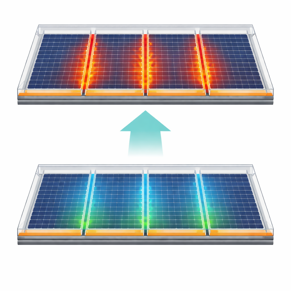
In the lab, single perovskite cells now reach power conversion efficiencies close to those of top silicon devices. Yet when the active area is enlarged to practical module sizes, efficiency falls and the devices age much faster. The researchers compared small cells with modules up to 100 square centimeters and found a clear pattern: while tiny devices stayed relatively stable, large modules degraded quickly, especially under long-term storage or light exposure. Careful imaging of aged modules revealed that failure nearly always began at the laser scribe lines used to divide and connect sub-cells, then spread into the surrounding light-absorbing film.
The Trouble Hidden in Fine Laser Cuts
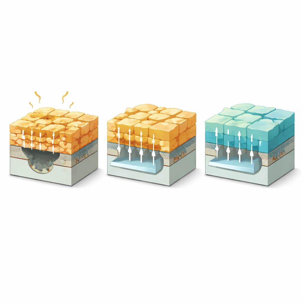
Modules are patterned with three main types of laser lines, known as P1, P2, and P3, each cutting different layers. At P1, the laser removes the transparent front electrode before any perovskite is deposited. The team found that these grooves create rough, uneven depressions that the underlying transport layer cannot fully fill. When the perovskite solution later dries and crystallizes over this landscape, solvent becomes trapped, crystals grow more slowly and unevenly, and microscopic voids and clumps of lead-rich material form. These weak spots degrade far faster than the flat regions between scribes, especially in humid air or under light.
Heat Damage from Connecting the Cells
The P2 and P3 scribes, made after the perovskite layer is in place, introduce a different problem: intense local heating. At P2, which cuts through the perovskite stack to expose buried electrodes, scanning microscopes showed melted splashes, rims of re-solidified material, and a thin, damaged layer along the edges. Chemical mapping revealed that the perovskite there partially breaks down, losing its organic component and leaving behind lead- and iodine-rich residues and oxides. At P3, where higher laser energy is needed to cut the metal back contact, the surrounding layers blur together and decompose even more severely, forming silver iodide and blocking efficient charge extraction. Together, these thermal scars become hotspots for long-term degradation.
Guiding Crystals from the Bottom Up
To tackle these weak regions, the researchers did not try to redesign the lasers themselves. Instead, they changed how the perovskite crystals form everywhere in the module, including inside the troublesome scribe depressions. They added a small amount of a molecule called BDECl to the precursor solution. This additive first forms an ultra-thin two-dimensional perovskite template at the bottom of the wet film. During heating, this template acts like a scaffold that encourages the main, three-dimensional perovskite to grow upward in an orderly, aligned fashion. As the film solidifies, the additive largely leaves, but its imprint remains in the form of tightly packed, well-oriented crystals with far fewer voids and defects.
Record Efficiencies and Longer Lifetimes
Modules made with this guided-growth strategy showed striking improvements. A seven-cell module of 25 square centimeters reached an efficiency of 24.70 percent, and a ten-cell 100-square-centimeter module achieved 23.89 percent, with an independently certified value of 23.55 percent—a record for this size class. Just as important, stability tests under light and in ambient air showed that unencapsulated modules kept over 90 percent of their original performance after thousands of hours, sharply outperforming conventional designs. By revealing how tiny laser lines can quietly undermine large-area perovskite modules, and demonstrating a practical way to harden these regions through smarter crystallization, the work brings high-efficiency, long-lived perovskite solar panels closer to everyday use.
Citation: Xie, Y., Fan, B., Li, H. et al. Regulating perovskite crystallization kinetics at laser scribe lines for efficient and stable perovskite modules. Nat Commun 17, 2977 (2026). https://doi.org/10.1038/s41467-026-69685-6
Keywords: perovskite solar modules, laser scribing, crystal growth, solar stability, additive engineering