Clear Sky Science · en
Precision engineering chiral interfaces for efficient spin injection in metal halide heterostructures
Twisting Light and Electrons
Modern electronics mostly cares about the charge of electrons. But every electron also behaves like a tiny spinning top. Devices that can tap into this “spin” promise faster, more efficient information technologies and ultrasensitive light detectors. This paper shows how carefully sculpting an invisible boundary only a few nanometers thick can dramatically improve how efficiently spinning electrons are injected from one material into another, all at room temperature. 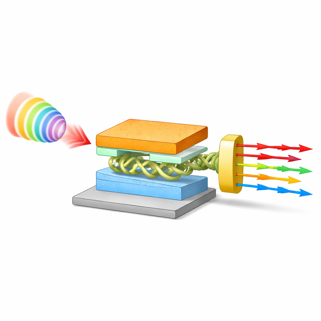
Why the Boundary Matters
When two different semiconductors touch, their shared boundary—called an interface—decides how well light-generated charges move and how much of their spin survives. In many promising “chiral” metal halide materials, molecules are arranged like tiny screws, naturally favoring one spin orientation over the other. This can, in principle, turn circularly polarized light into spin-polarized current without magnets. In practice, however, the interfaces between chiral and ordinary semiconductors often introduce strain and defects that scramble spins before they can be used, limiting the performance of spin-based photodetectors and solar-like devices.
Building a Gentle Helical Bridge
The authors tackle this by growing a specially twisted, or helical, layer of lead iodide (called R-PbI2) exactly at the interface between a chiral perovskite (R-NEAPbI3) and ordinary PbI2. They spin-coat a precursor film and then carefully heat it so that most of the perovskite converts to regular PbI2, while a very thin R-PbI2 layer emerges in between. Advanced measurements, including X-ray diffraction and high-resolution electron microscopy, confirm that this interlayer adopts a helical distortion that mirrors the chirality of the perovskite beneath it. Crucially, this interlayer reduces the mismatch in atomic spacing between the two bulk materials, easing mechanical strain and cutting the density of electronic defects to roughly one-third of that in a similar structure lacking the helical bridge.
Following Excitons and Spins in Motion
To see how this engineered interface affects light-generated quasiparticles, the team uses ultrafast pump–probe spectroscopy. They first study how excitons—electron–hole pairs created by a light pulse—form and decay. In structures with the helical R-PbI2 layer, these excitons live longer than in a comparison sample, signaling cleaner interfaces with fewer traps. Next, they track spin dynamics using circularly polarized pulses, which create excitons with a defined spin, and circularly polarized probes that read out how that spin decays over trillionths of a second. Despite similar initial spin polarization in both types of samples, only the structure with the chiral interlayer shows a strong, long-lived imbalance between spin “up” and spin “down” populations under conditions where the pump light itself does not imprint spin. This reveals that the interface is acting as a spin-selective gateway, preferentially transferring one spin orientation across the boundary. 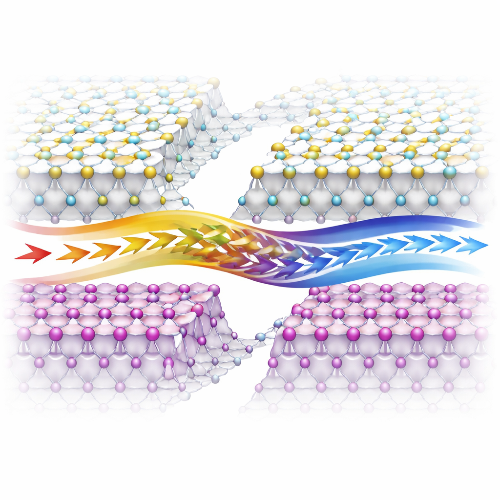
Turning Spin Control into a Working Device
To translate this microscopic behavior into a practical outcome, the researchers build a spin-photovoltaic device where the chiral heterostructure sits between charge-transport layers and metal contacts. When they shine right- or left-circularly polarized light tuned to excite the PbI2 region, the device with the engineered chiral interface produces a photocurrent whose magnitude differs by nearly 30 percent depending on the light’s handedness—about twice the polarization achieved in earlier chiral perovskite devices. By combining this measurement with knowledge of the initial light-induced spin and the chiral perovskite’s filtering ability, they deduce that up to 68 percent of the spin polarization survives crossing the interface, a record value for such materials.
What This Means for Future Technologies
For non-specialists, the key message is that the authors learned to “soften” a harsh boundary between two crystals by inserting a nanoscopic, twisted bridge that shares structural traits with both sides. This smoother, chiral interface lets electrons keep their spin orientation as they move, which translates directly into a stronger electrical response to circularly polarized light at room temperature. Although the overall current polarization is still limited by spin loss inside the bulk PbI2, the work shows that carefully engineered interfaces can dramatically boost spin injection. Such strategies could underpin future spin-based photodetectors, light-emitting devices, and information processors that are more efficient and tunable than conventional electronics.
Citation: Xiao, J., Li, Y., Liu, Y. et al. Precision engineering chiral interfaces for efficient spin injection in metal halide heterostructures. Nat Commun 17, 2969 (2026). https://doi.org/10.1038/s41467-026-69455-4
Keywords: chiral perovskites, spintronics, circularly polarized light, heterostructure interfaces, spin-photovoltaic devices