Clear Sky Science · en
Heterogeneous integration of micro-LEDs via multiple simultaneous transfer and bonding
Why tiny new lights matter
Televisions, smart watches, and virtual reality headsets increasingly rely on tiny light sources called micro LEDs to create brighter, sharper, and more power efficient screens. But building these displays has been slow and expensive, mainly because it is hard to move and connect millions of microscopic light chips onto the electronics that control them. This study presents a new way to transfer and attach many different kinds of micro LEDs to one display panel quickly and reliably, which could help bring high quality full color micro LED screens into everyday products.
A new way to move and attach chips
The researchers developed a process they call multiple simultaneous transfer and bonding, or SITRAB, that handles both moving the chips and making their electrical connections in a single step. A thin film of a specially designed adhesive is first laminated onto a display backplane that already carries tiny metal solder bumps. Arrays of micro LED chips, held on transparent rubberlike carriers, are carefully aligned above the matching electrodes. When an infrared laser shines through the carrier for a few seconds while gentle pressure is applied, the heat activates the adhesive and melts the solder so that each chip becomes firmly bonded and electrically connected to the panel underneath. When the carrier is lifted away, the chips remain on the display in their precise pattern. 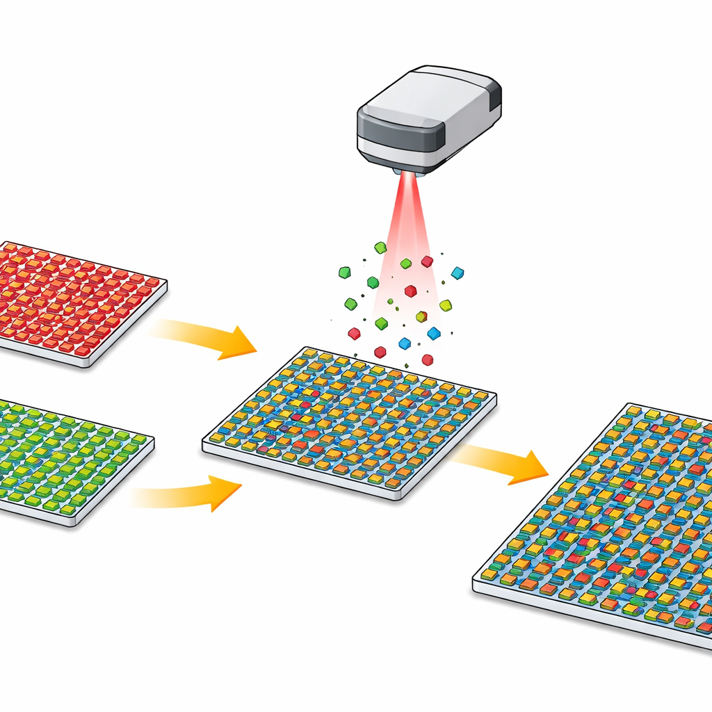
Adhesive that can work again and again
A key challenge in micro LED manufacturing is that most bonding materials harden permanently after one heating step, which prevents adding more chips later or repairing faulty ones. The SITRAB adhesive is different. It is made from epoxy, a carboxylic acid, and an imidazole based catalyst, blended so that it can clean the solder surface, flow into gaps, and protect the joints while still surviving repeated laser exposure. Using chemical analysis, the team showed that the main active groups in the adhesive remained intact even after six laser shots, meaning its soldering ability was preserved. Only when the material was baked in a conventional oven at higher temperature did these groups fully cure, so the process window can be carefully controlled.
Sharp images and sturdy connections
To test how well this method works in real devices, the team transferred red, green, and blue micro LEDs made from different semiconductor stacks onto glass and silicon backplanes. Microscopy images revealed dense, well formed solder joints between the gold pads on the chips and indium based bumps on the panel, with the adhesive neatly filling the surrounding space like an invisible cushion. Electrical measurements showed that the current–voltage behavior of the LEDs barely changed after transfer, and the lights operated smoothly up to current levels much higher than those needed in typical displays. Optical tests confirmed bright red, green, and blue emission covering more color range than standard television formats require, and the devices kept their performance even after high temperature, humidity, and thermal cycling tests.
Building bigger and fixing flaws
Because SITRAB can be repeated with the same adhesive layer, it becomes possible to assemble displays in modules and to repair defects. The authors demonstrated “stitching” together four separate 15 by 15 micro LED arrays onto one backplane to form a larger 30 by 30 pixel area, and extended this to hundreds of pixels on a six inch panel. They also designed backplanes with extra repair electrodes in each pixel. After an initial transfer from a partially defective source array, they identified dark pixels and then used an additional SITRAB step to place spare LEDs onto the repair pads, dramatically boosting the working pixel yield from about 83 percent to nearly 99.8 percent without having to remove any of the original chips. 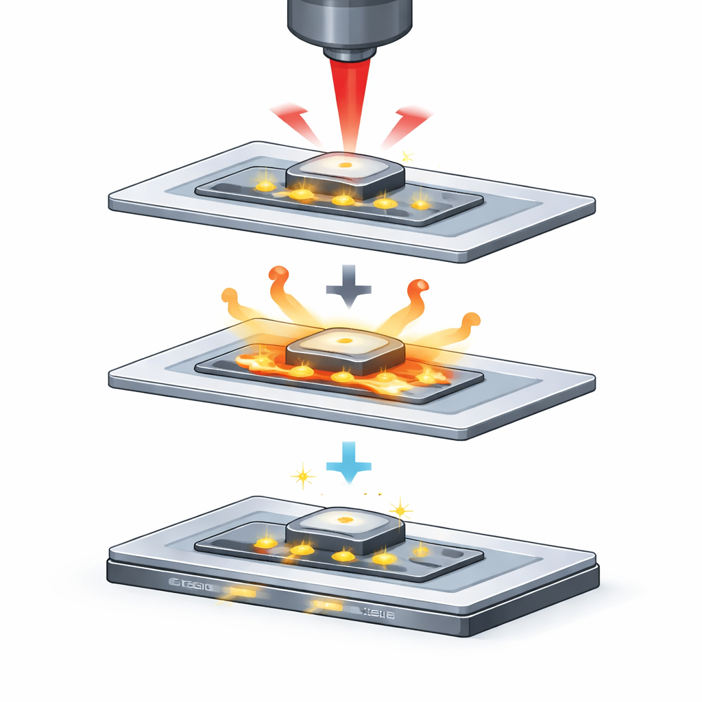
Full color displays from mixed parts
Finally, the researchers used multiple SITRAB steps to assemble full color pixels by adding red, green, and blue micro LEDs from three different carriers onto the same glass backplane. Despite slight differences in chip thickness, the process maintained accurate alignment so that the three colored subpixels in each pixel sat just tens of micrometers apart. Cross sectional imaging showed clean solder joints for all colors, and when driven together, the combined arrays could display white light and full color patterns at a resolution suitable for early micro LED panels. This proof of concept suggests that manufacturers could one day mix and match micro LEDs with different materials, sizes, and functions on a single panel.
What this could mean for future screens
In everyday terms, this work offers a more flexible, repairable, and scalable way to build tiny light engines for next generation displays. By using a laser friendly adhesive that stays active through several bonding cycles, the SITRAB method lets engineers tile small LED blocks into larger screens, replace bad pixels, and combine red, green, and blue chips from separate sources without redoing the bonding layer. While more development is needed to reach the resolutions of phone and watch screens, the approach addresses several practical bottlenecks in micro LED manufacturing and could also be adapted to other light emitting devices such as quantum dot based emitters and organic LEDs.
Citation: Joo, J., Choi, GM., Lee, C. et al. Heterogeneous integration of micro-LEDs via multiple simultaneous transfer and bonding. Microsyst Nanoeng 12, 170 (2026). https://doi.org/10.1038/s41378-026-01304-2
Keywords: micro LED displays, laser bonding, adhesive interconnection, display repair, full color pixels