Clear Sky Science · en
Interface defect engineering enables high-performance lead-free perovskite photodetectors with an ultrafast response and broadband sensitivity
Why Faster, Safer Light Sensors Matter
From smartphone cameras to medical scanners and self-driving cars, devices that sense light are everywhere. Many of today’s best light detectors rely on materials that contain toxic lead, creating environmental and health concerns. This study introduces a new way to build flexible, highly sensitive light sensors that avoid lead, yet still react extremely quickly and work across a wide range of colors—from ultraviolet to near‑infrared. The work points toward safer, bendable detectors for future imaging, communication, and wearable technologies.
Building a Safer Light-Harvesting Stack
The researchers start with a special class of crystals called perovskites, which are excellent at soaking up light and turning it into electrical charge. Instead of using lead-based versions, they choose a tin-based material known as FASnI3, which is much less toxic but harder to make perform well. They coat this light-harvesting film onto a flexible plastic sheet and then add a thin layer of another material, InGaZnO, on top. The bottom layer acts like a sponge for incoming light, while the top layer behaves as a clean highway for the freed charges to travel along, forming a stacked structure that can bend without losing function. 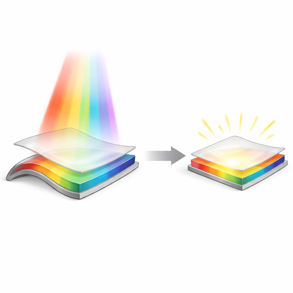
Turning Tiny Imperfections into an Advantage
Normally, defects—tiny imperfections in a material—are bad news for electronics because they trap charges and waste energy. In this work, the team deliberately engineers the interface between the two layers so that certain defects actually help. During the process of depositing the InGaZnO layer, energetic argon gas disrupts weak chemical bonds in the perovskite, allowing hydrogen atoms to slip into the boundary and form new bonds with tin and iodine. These microscopic changes create well‑placed “parking spots” for electrons right at the junction between the layers. Instead of randomly slowing the device, these controlled traps are positioned so they can briefly hold electrons and influence the current in the upper channel in a predictable, beneficial way.
Balancing High Sensitivity with Speed
A common tradeoff in light detectors is that devices which are extremely sensitive often react sluggishly: they collect and hold charges for a long time, which boosts the signal but slows the response. The new design breaks this compromise. When light shines on the device, the perovskite layer generates electrons and holes. Thanks to the energy landscape at the junction, many electrons quickly move into the InGaZnO layer and dramatically increase its conductivity, while others are caught by the engineered traps at the interface. These trapped electrons act like an invisible gate that keeps the upper channel in a highly conductive state, greatly amplifying the signal. Once the light is turned off, the trapped electrons are released in a controlled way, allowing the channel current to fall back to its dark level within a few thousandths of a second—orders of magnitude faster than many earlier lead‑free perovskite detectors. 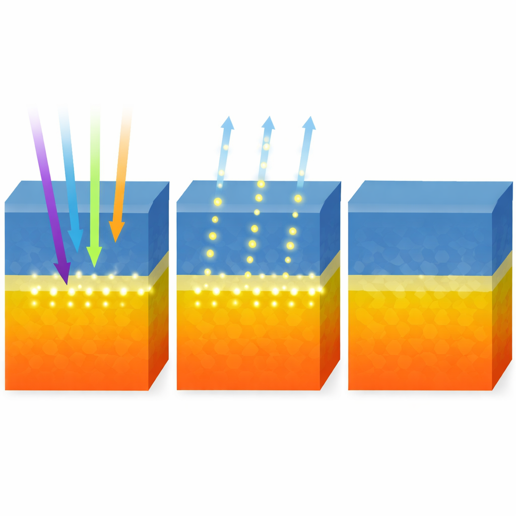
Seeing More Colors with Less Noise
Because of the way charges move and are stored in this stacked structure, the device can detect very weak light and distinguish it cleanly from background electrical noise. It achieves high responsivity, meaning it produces a strong electrical output even for small amounts of light, and excellent detectivity, which reflects how well it can pick out faint signals. Remarkably, it responds to wavelengths from the near‑ultraviolet through the visible spectrum and deep into the near‑infrared, beyond the main absorption edge of the perovskite itself. The researchers suggest that deeper‑color sensitivity may come from exciting charges out of defect states within the material, extending the usable range for applications like night‑vision imaging or optical communication.
Bendable Devices for Future Wearables
The team also tests how the sensors behave when bent and flexed, an important step toward wearable or foldable electronics. Mounted on a flexible plastic film, the detectors maintain nearly the same performance even when curved to large angles and repeatedly cycled hundreds of times. A 20-by-20 array of these pixels can map simple images, such as a shaped light pattern, before and after bending with minimal variation from pixel to pixel. This robustness suggests that the technology could be scaled up into flexible imaging sheets that conform to curved surfaces.
What This Means Going Forward
By carefully controlling defects at the interface between a light‑absorbing tin perovskite and a transparent semiconductor channel, the researchers have built a lead‑free photodetector that is both highly sensitive and extremely fast, while remaining thin, flexible, and stable. To a non‑specialist, the key message is simple: instead of treating imperfections as a problem to eliminate, this work turns them into a tool, solving a long‑standing tradeoff between speed and sensitivity in safer, more environmentally friendly light sensors. This strategy could guide the design of next‑generation cameras, wearable monitors, and communication devices that see more, react faster, and are kinder to the planet.
Citation: Qianlei Tian, Zhen Liu, Yuan Zhou, Sen Zhang, Xitong Hong, Chang Liu, Xingqiang Liu, Zhongzheng Wang, Yawei Lv, Lei Liao, and Xuming Zou, "Interface defect engineering enables high-performance lead-free perovskite photodetectors with an ultrafast response and broadband sensitivity," Optica 12, 1757-1764 (2025). https://doi.org/10.1364/OPTICA.573280
Keywords: lead-free perovskite, photodetector, flexible electronics, broadband imaging, optoelectronic devices