Clear Sky Science · en
Embedded growth of visible InP quantum dot lasers in silicon nitride photonic integrated circuits
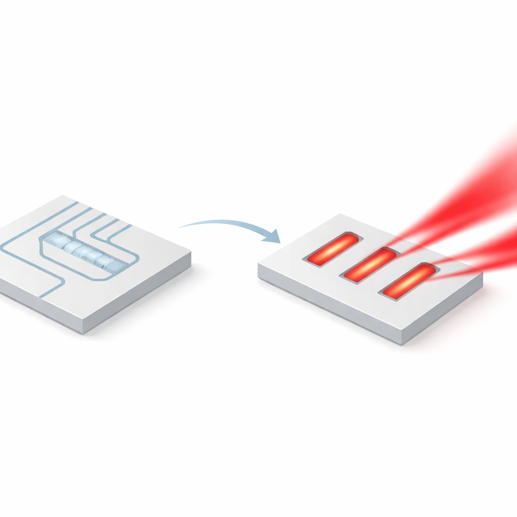
Bringing Red Light Onto a Chip
Many of tomorrow’s technologies—from quantum computers to ultra-small medical sensors and next‑generation displays—depend on tiny, efficient light sources that can live directly on a computer chip. This paper shows how researchers have grown bright red‑emitting lasers directly inside a silicon‑based photonic circuit, pointing the way toward compact, low‑cost optical chips that work at visible wavelengths instead of just the infrared used in today’s data centers.
Why Visible Light on Chips Matters
Standard silicon chips are great at handling electrical signals but do a poor job guiding visible light because silicon absorbs it. A closely related material, silicon nitride, is transparent across a wide range of colors, including much of the visible spectrum, and can be fabricated using the same large‑scale manufacturing tools as conventional electronics. If reliable light sources could be built directly on silicon nitride photonic circuits, a single chip might route, split and process beams of light for quantum information, analyze biological samples by their optical fingerprints, or project images for augmented‑reality displays. Until now, however, most on‑chip lasers grown directly on silicon have operated at infrared wavelengths, and visible red lasers have been especially challenging to integrate.
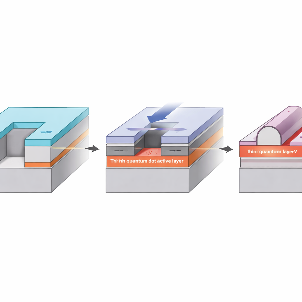
Growing Tiny Red Lasers in Microscopic Pockets
The team tackles this by carving narrow “pockets” into a silicon nitride photonic circuit and then growing the laser material only inside those recessed regions. At the base sits a silicon wafer, topped by a thin germanium layer that helps relieve crystal strain and reduce defects. Above that, layers of glass and silicon nitride form low‑loss waveguides. The researchers etch trenches down through these layers until they expose the germanium, then selectively grow high‑quality gallium arsenide inside the pockets. Finally, they use molecular beam epitaxy—a precise vapor‑phase growth method—to deposit stacks of semiconductor layers that form the heart of the laser.
Harnessing Quantum Dots for Stable Red Light
At the core of each device is an active region made from indium phosphide quantum dots embedded in carefully engineered surrounding layers. Quantum dots are nanometer‑scale islands that confine electrons and holes so strongly that they behave like artificial atoms, which can improve efficiency and make devices more tolerant to crystalline imperfections. Microscopy measurements show dense, well‑formed quantum dot layers within the grown structure, while optical tests after a rapid thermal annealing step reveal strong red emission around 745–752 nanometers, squarely in the deep‑red part of the spectrum. Although temperature control during growth is complicated by the patterned wafer, the team still achieves a dot density and optical quality competitive with the best reported structures on simpler substrates.
Performance of the On‑Chip Red Lasers
After defining narrow ridges and cleaving the ends of the devices to act as mirrors, the researchers test the completed edge‑emitting lasers under continuous‑wave electrical drive at room temperature. They report a remarkably low threshold current density—how much electrical current is needed per unit area to start lasing—of 450 amperes per square centimeter, and more than 10 milliwatts of output from a single facet, despite not yet coupling light into the silicon nitride waveguides. These thresholds are significantly lower than comparable red quantum dot lasers previously grown on silicon, and the overall efficiencies match earlier devices made on more ideal, unpatterned templates. The lasers continue to emit milliwatt‑level power up to about 50 °C, with thermal behavior similar to other state‑of‑the‑art red quantum dot lasers.
What This Means for Future Photonic Chips
In plain terms, the study shows that bright, efficient red lasers can be grown directly inside the fabric of a silicon nitride photonic circuit without sacrificing performance. While this work stops short of demonstrating full optical coupling into the waveguides, it validates the key step: embedding high‑quality visible‑wavelength gain material in foundry‑processed chips. With future refinements—such as etched mirrors for mass production and improved thermal design—this approach could enable densely packed visible‑light photonic integrated circuits, powering applications from biosensors and quantum processors to compact display and sensing systems that fit on a single chip.
Citation: Yiteng Wang, Christopher Heidelberger, Jason Plant, Dave Kharas, Pankul Dhingra, Robert B. Kaufman, Xizheng Fang, Brian D. Li, Ryan D. Hool, John Dallesasse, Paul W. Juodawlkis, Cheryl Sorace-Agaskar, and Minjoo Larry Lee, "Embedded growth of visible InP quantum dot lasers in silicon nitride photonic integrated circuits," Optica 12, 1697-1701 (2025). https://doi.org/10.1364/OPTICA.569454
Keywords: silicon nitride photonics, visible lasers on silicon, quantum dot lasers, integrated photonic circuits, red light sources