Clear Sky Science · en
Manipulating the intrinsic light–matter interaction with high-Q resonances in an etch-free van der Waals metasurface
Turning Dim Materials into Bright Light Tools
Many of the most exciting ideas in nanotechnology and quantum devices rely on getting light and matter to interact as strongly as possible. This paper shows a new way to do that using ultra-thin, stackable crystals known as van der Waals materials—without the harsh etching steps that usually damage them. By gently patterning only a soft coating on top, the authors create a versatile “metasurface” that can dramatically sharpen, steer, and strengthen light inside a wide range of 2D semiconductors, opening doors to better sensors, light sources, and quantum components.
A Gentle Way to Shape Light
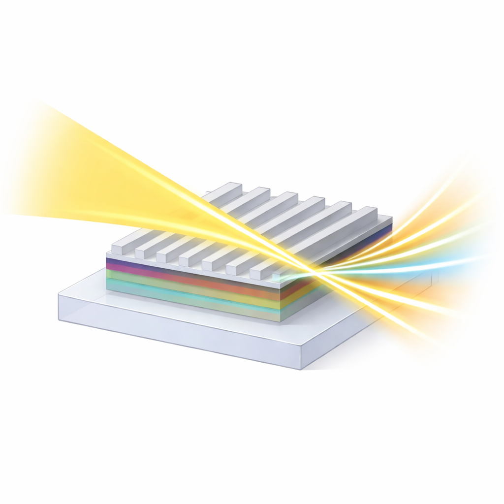
Conventional nanophotonic devices often rely on carving tiny features directly into the active material with reactive etching, a process that is difficult to control and can degrade fragile crystals. This is especially problematic for layered van der Waals materials such as WS2 and MoSe2, whose atomic-scale surfaces and sidewalls are easily damaged. The authors propose an alternative: leave the functional material intact and instead add a patterned layer of low-index photoresist—essentially a transparent polymer—on top. This patterned top layer forms a grating that slightly disturbs the way light propagates in the high-index crystal underneath, converting internal guided waves into sharp optical resonances known as guided-mode resonances and bound states in the continuum. Because the polymer is low-index and only weakly perturbs the crystal, scattering losses are reduced and the underlying material remains chemically pristine.
High-Quality Resonances Without the Damage
Using this etch-free strategy, the team fabricates simple grating patterns on bulk flakes of several transition metal dichalcogenides. They show that the polymer grating can mimic what would happen if the crystal itself were shallowly etched, but with cleaner optical behavior. Carefully tuning the period, thickness, and duty cycle of the grating lets them engineer very narrow resonances, quantified by a quality factor. They measure Q values up to about 348 in WS2, comparable to the best etched devices that require far more delicate and asymmetric nanostructures. Simulations indicate that even higher Qs, above a thousand, are possible. Crucially, the strongest fields of these modes reside inside the van der Waals layer itself, so the material’s electrons and excitons feel the full impact of the enhanced light.
Hybrid Light–Matter States and Brightened Emission
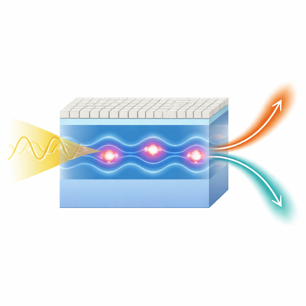
When the engineered optical resonances are tuned to lie near the natural exciton energies of the materials, the photons in the cavity and the excitons in the crystal strongly mix, forming hybrid particles called polaritons. The authors observe such self-hybridized polaritons in four different semiconductors: WS2, MoS2, WSe2, and MoSe2. In WS2 and MoSe2, they clearly see an “anticrossing” pattern in angle-resolved transmission experiments, a hallmark of strong coupling, with energy splittings of around 80 and 72 millielectronvolts—larger than the natural linewidths of the excitons. Beyond this strong-coupling physics, the high-Q modes are used to amplify otherwise weak light emission channels. For thick WS2, which normally emits very inefficient, phonon-assisted indirect light, the etch-free cavity boosts the emission by roughly 25 times and narrows its spectral width. Time-resolved measurements show that the cavity speeds up radiative recombination and increases the fraction of excitations that emit photons, while angle-resolved data reveal that the structure also funnels light into directions that are more easily collected.
From Single Layers to Complex Stacks
The approach is not limited to single bulk crystals. The authors also build a heterostructure in which a monolayer of MoSe2 is sandwiched between two layers of hexagonal boron nitride and then overlaid with a polymer grating. In this configuration the active monolayer sits directly inside the optical mode volume. As the resonance is tuned across the exciton energy, they observe clear dips in transmission and a three- to five-fold enhancement of the bright exciton emission when the polarization matches the cavity mode. Although this device does not yet reach the strong-coupling regime—limited by interface roughness, residual contamination from fabrication, and the lower index of boron nitride—it demonstrates that the same etch-free philosophy can be applied to more complex stacks, bringing direct excitons and cavity modes into intimate contact without cutting into the active layers.
Why This Matters for Future Devices
In essence, this work provides a “universal socket” for enhancing and controlling light–matter interaction in almost any van der Waals material or heterostructure. By offloading all patterning to a benign, removable top layer, the method sidesteps the chemical reactivity and structural damage that have limited earlier metasurfaces. It delivers high-Q resonances, strong polariton formation, and large, polarization-dependent boosts in emission from both indirect and direct bandgap transitions, all while preserving material integrity. This gentle yet powerful design strategy is well suited to emerging layered magnets, nonlinear crystals, and exotic low-symmetry materials, and could help transform fragile atomic-thin films into robust building blocks for next-generation photonics and quantum technologies.
Citation: Fuhuan Shen, Dayou Liu, Zefeng Chen, Jiasen Zhu, Shuaiyu Jin, Xinyi Zhao, Yungui Ma, Dangyuan Lei, and Jianbin Xu, "Manipulating the intrinsic light–matter interaction with high-Q resonances in an etch-free van der Waals metasurface," Optica 12, 1702-1711 (2025). https://doi.org/10.1364/OPTICA.562661
Keywords: van der Waals metasurfaces, guided-mode resonance, exciton polaritons, etch-free nanophotonics, transition metal dichalcogenides