Clear Sky Science · en
Recent advances in ultra-precision manufacturing of electronic, photonic and quantum devices
Tiny Machines, Big Impact
Every year our phones, computers, and sensors get faster, smaller, and more powerful. Behind that quiet revolution lies a hidden world of manufacturing where engineers must shape and polish materials with accuracy measured in atoms. This article explains how a new generation of ultra-precision manufacturing methods is making that possible, and why they are essential for tomorrow’s electronics, photonics, and quantum devices that will power communications, medical tools, and even future quantum computers.

From Handcrafted Optics to Atomic Perfection
Ultra-precision manufacturing began decades ago in the optics industry, when researchers needed mirrors and lenses so smooth that tiny imperfections would not blur infrared images. Innovations such as air-bearing spindles and diamond-tipped tools replaced skilled hand polishing with highly controlled cutting and grinding. As electronic chips shrank and new technologies like high-speed communication and laser-based sensing emerged, the same demand for flawless surfaces and exact dimensions spread from optics to semiconductor wafers, tiny mechanical devices, and quantum hardware. Today, the goal is not just smoothness you can feel, but smoothness on the scale of a fraction of a nanometer—thousands of times smaller than a speck of dust.
Many Tools Working as One
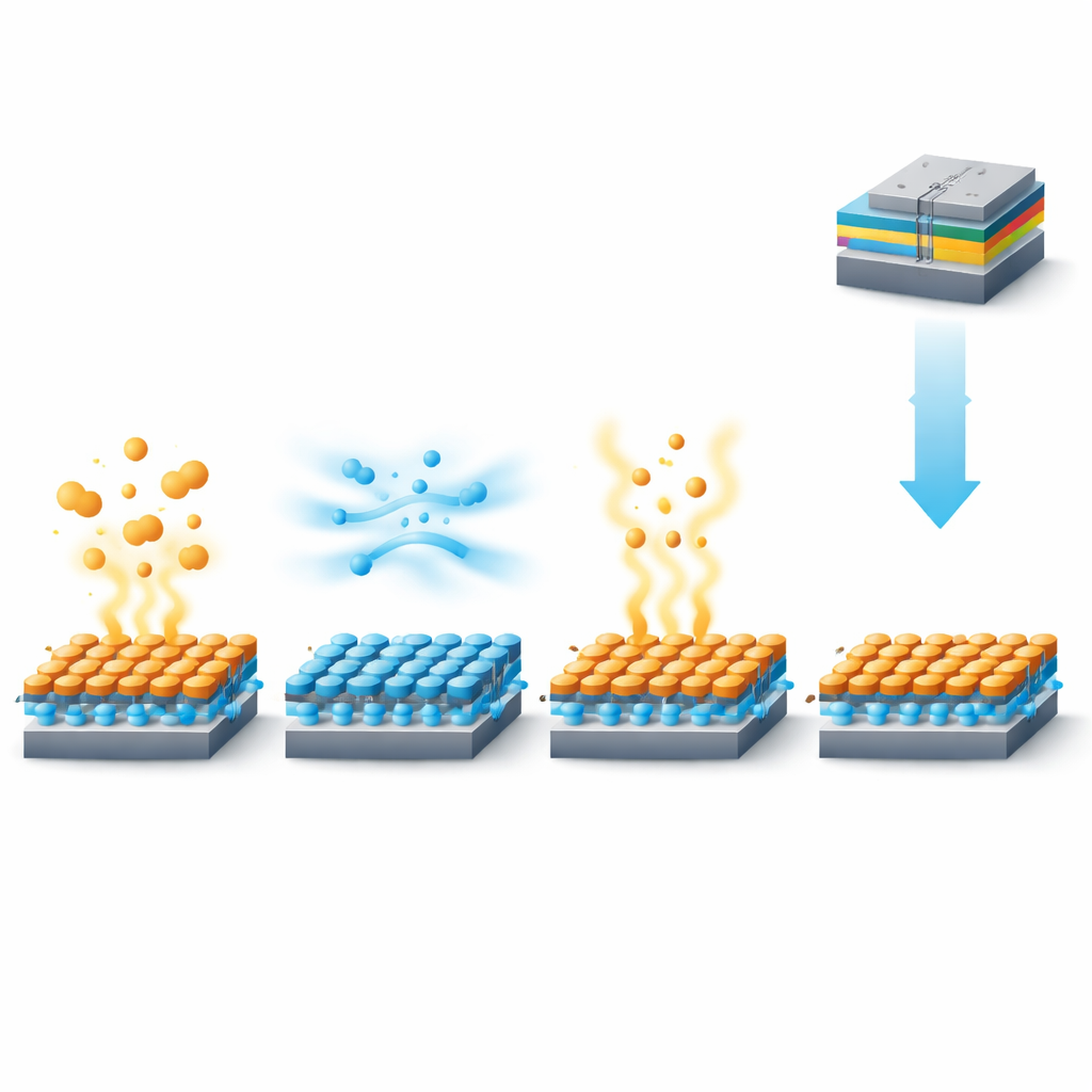
No single tool can do everything at these scales, so modern factories combine several families of processes, each playing a different role. Mechanical techniques such as ultra-precision diamond turning and fine grinding are used to carve the overall shape of lenses, housings, and wafers with extraordinary accuracy. Laser and ion-beam methods then step in to refine local details without touching the surface, using pulses of light or charged particles to gently remove material atom by atom. Chemical approaches such as atomic layer deposition and atomic layer etching build up or peel away films one molecular layer at a time, enabling perfect interfaces inside advanced chips and quantum circuits. Additive methods, including nanoscale 3D printing, are merged with careful polishing to create intricate three-dimensional structures that would be impossible with cutting alone.
Seeing, Measuring, and Guiding Every Step
Working at atomic scales is only possible if you can measure what you are doing. The review highlights how metrology—precision measurement—has become an active partner rather than a final inspection step. Optical interferometers, scanning probe microscopes, and advanced X-ray techniques can track tiny changes in shape, roughness, and internal strain. Increasingly, sensors are built directly into machines so that surfaces can be monitored while they are being made. Streams of data from optical, thermal, and acoustic sensors are combined and interpreted by artificial intelligence systems, which learn how tool wear, temperature drift, and subtle vibrations affect the outcome. Digital “twins” of the machines—virtual replicas running side by side with the real hardware—use this information to predict problems before they happen and adjust settings on the fly.
Smarter Factories for Chips, Light, and Qubits
These capabilities are already reshaping industries. In microelectronics, ultra-precision methods are used to keep entire wafers flat within a few nanometers, smooth the walls of ever-shrinking metal lines, and bond stacked chips with nearly perfect alignment for three-dimensional circuitry. In photonics, they create waveguides and tiny resonators whose surfaces are so clean that light can circulate with almost no loss. Quantum devices, from superconducting circuits to solid-state qubits, rely on exquisitely engineered surfaces and interfaces to maintain fragile quantum states. Micro- and nano-electromechanical sensors benefit from uniform thickness and stress, while flexible electronics and wearable optics depend on clean, well-bonded layers across soft, bendable substrates.
Roadblocks, Green Goals, and the Next Leap
Despite impressive progress, major challenges remain. The most precise techniques tend to be slow and expensive, making it difficult to scale them to large wafers or high production volumes. Tools gradually wear out, temperatures drift, and tiny contaminants can ruin otherwise perfect devices. The article argues that the real frontier is achieving “precision at scale” by combining multiple processes in smart chains, parallelizing operations, and using AI and digital twins to keep quality stable over long runs. At the same time, there is growing pressure to cut energy use, waste, and reliance on rare materials, prompting research into greener coolants, recyclable tools, and low-energy lasers. Looking ahead, the authors envision autonomous, self-calibrating manufacturing cells equipped with quantum-enhanced sensors, capable of controlling matter at the atomic level reliably, affordably, and sustainably. For everyday users, that future will appear as smaller, more capable, and more efficient devices woven seamlessly into daily life.
Citation: Verma, J., Ameli, N., Kumar Katiyar, N. et al. Recent advances in ultra-precision manufacturing of electronic, photonic and quantum devices. npj Adv. Manuf. 3, 13 (2026). https://doi.org/10.1038/s44334-026-00074-z
Keywords: ultra-precision manufacturing, atomic-scale fabrication, semiconductor processing, photonics and quantum devices, AI in manufacturing