Clear Sky Science · en
Inverse design and 3D printing of a multiport microwave power splitter: a scalable electromagnetic design framework
Smarter Building Blocks for High-Speed Signals
Our phones, radar systems, satellites and even factory sensors all rely on invisible high‑frequency waves to send and measure information. Inside this hardware sit small components that quietly manage how power is split and routed between different paths. This paper shows how computers and 3D printing can team up to design one of these workhorses—a microwave power splitter—in a way that is more flexible, more adaptable and easier to manufacture than traditional approaches.
Why Splitting Power Matters
In many radio and microwave systems, a single incoming signal must be divided among several outputs. For example, phased‑array antennas use many tiny elements whose combined output forms steerable beams, and test equipment often needs to feed the same signal into multiple measuring channels. Today, engineers usually rely on a small set of standard circuit layouts, such as Wilkinson dividers or branch‑line couplers, that were worked out decades ago. These tried‑and‑true designs work well for simple cases, but they become awkward when many ports are needed, when space is tight, or when the splitter must fit an unusual shape inside a larger system. Designers end up chaining standard parts together and tweaking them by trial and error, which is slow and can miss better solutions.
Letting the Computer Draw the Circuit
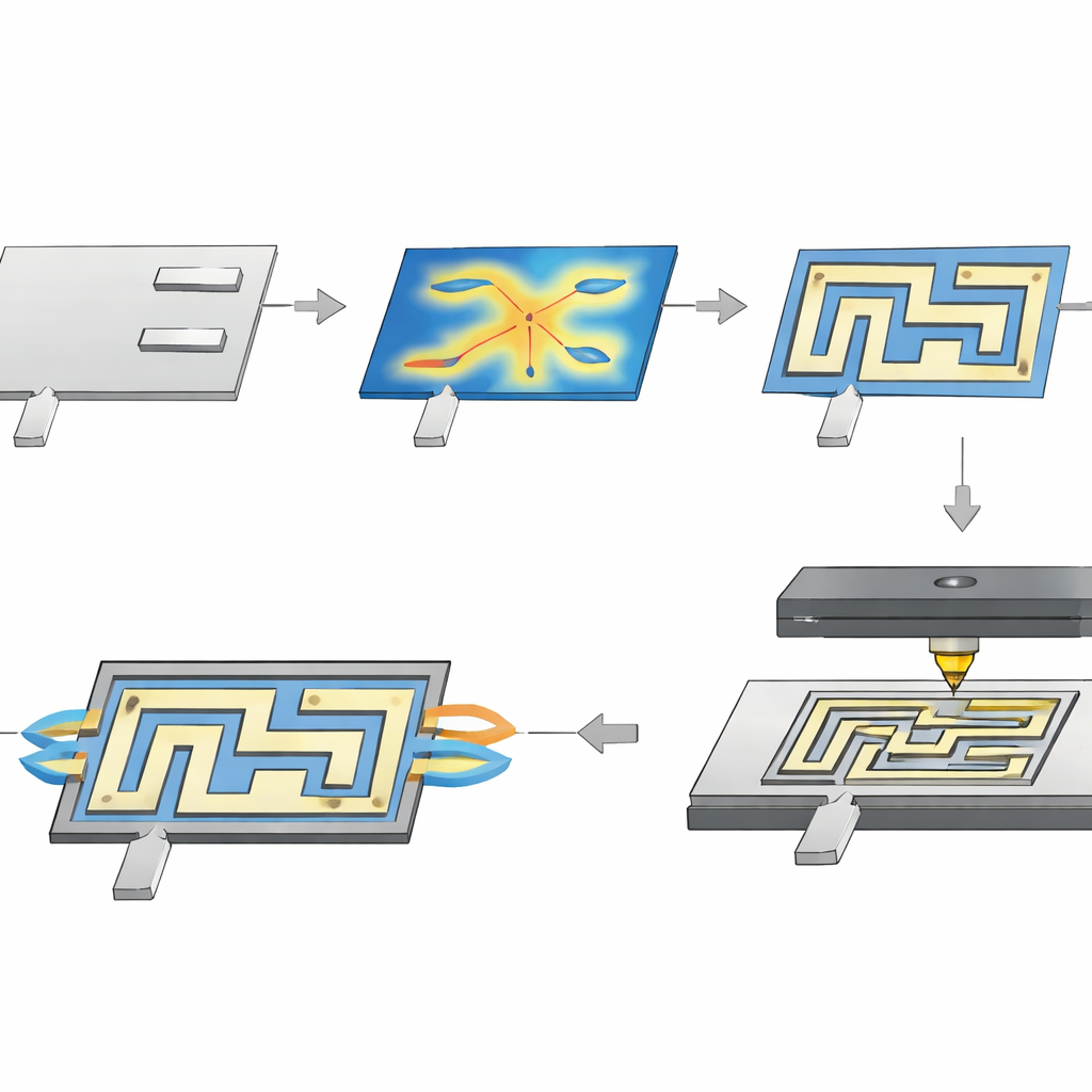
The authors replace this manual tuning process with an “inverse design” strategy. Instead of starting from a known circuit shape, they begin by writing down what they want the device to do: how much power should emerge from each output, how little should bounce back to the input, and how strongly one port should be isolated from another. They then let an optimization algorithm adjust a grid of material inside a design region until computer simulations of the electromagnetic fields show that these targets are being met. A mathematical shortcut called the adjoint method makes this search efficient: it extracts how every pixel in the device should change to improve performance from only a couple of simulations, rather than thousands. Because the algorithm manipulates a continuous pattern of material rather than a fixed circuit template, it can explore unusual shapes that a human designer might never think to draw.
Designing with the Factory in Mind
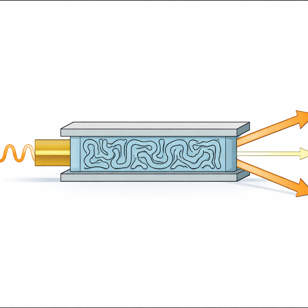
Crucially, the method is built to respect how the part will actually be made. The team chooses a commercial 3D‑printing process known as Multi Jet Fusion, which builds thin layers of nylon powder into solid shapes. They bake printer limits directly into the design rules by enforcing a minimum feature size, controlling how sharply corners can turn, and filtering out tiny details that the printer cannot reliably reproduce. The device itself is a flat nylon insert with a maze‑like pattern of dielectric material, sandwiched between two metal plates that guide the microwave fields. Because the same optimization code only needs simple geometric limits and a basic material description, it can be adapted to other printers or machining methods without rewriting the underlying physics.
Putting the New Splitter to the Test
To demonstrate the approach, the researchers design a four‑port power splitter that operates around 10 gigahertz, a common microwave band. In simulations, they tune the internal pattern so that power entering one port is routed equally to two others while almost none leaks to the remaining “isolation” port. After printing and assembling the device, they measure its performance with a network analyzer. The real‑world results closely track the simulations: reflections back into the input are low, the two output ports share the power fairly evenly, and unwanted coupling into the isolated port stays well suppressed. The splitter works over a fractional bandwidth of about 23%, which is wider than many classic four‑port couplers, though its loss is somewhat higher because the printed polymer is not as low‑loss as specialized circuit materials.
A Flexible Blueprint for Future Devices
While the paper focuses on one four‑port splitter, the authors stress that the real advance is the design recipe itself. Because performance goals are written directly in terms of field behavior at the ports, and because manufacturing limits are handled in a general way, the same framework can be extended to devices with more ports, different power‑sharing ratios or entirely different roles such as filters and antennas. In the longer term, the same tools could even handle tunable or active parts by allowing material properties to change. For readers outside microwave engineering, the key message is that combining physics‑aware optimization with practical 3D printing can turn a difficult, intuition‑driven craft into a scalable, programmable process for shaping how waves move through space.
Citation: Zolfaghary Pour, S., Zhang, H., Liu, P.W. et al. Inverse design and 3D printing of a multiport microwave power splitter: a scalable electromagnetic design framework. Commun Eng 5, 53 (2026). https://doi.org/10.1038/s44172-026-00601-y
Keywords: inverse design, microwave power splitter, adjoint optimization, 3D printing, multiport RF devices