Clear Sky Science · en
Deep learning modeling of oxygen redistribution and thermal transport in silicon on insulator and buried oxide layers
Why this matters for everyday electronics
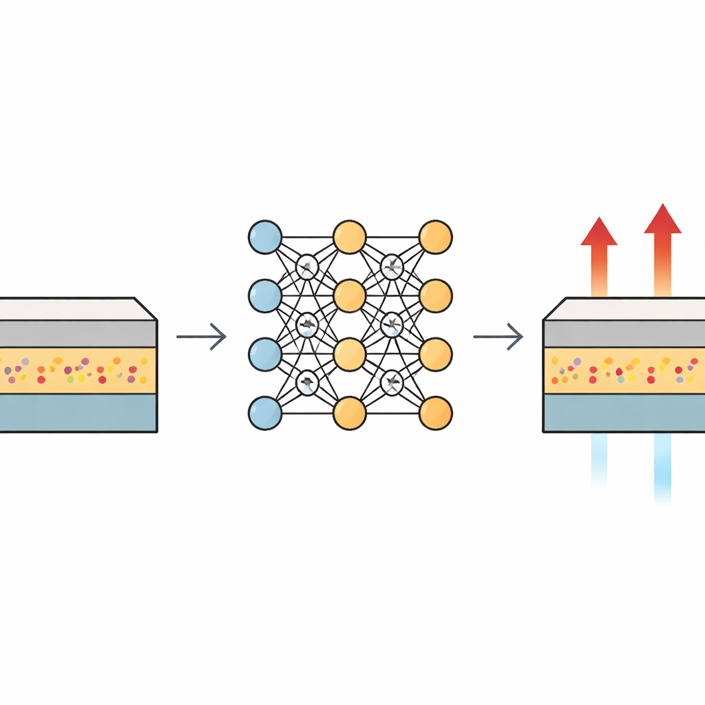
From smartphones to data centers, many fast and energy‑efficient chips rely on a special kind of silicon wafer called “silicon on insulator.” In these wafers, an ultra‑thin silicon layer sits on top of a buried glass‑like layer that helps keep heat and electrical noise under control. Building these structures requires driving oxygen deep into hot silicon and then managing how heat sneaks across the boundaries between materials. The paper behind this summary shows how advanced artificial intelligence can predict both the hidden oxygen patterns and the way heat flows at these buried interfaces, offering a powerful new design tool for future high‑performance electronics.
How chips are built on hidden glass layers
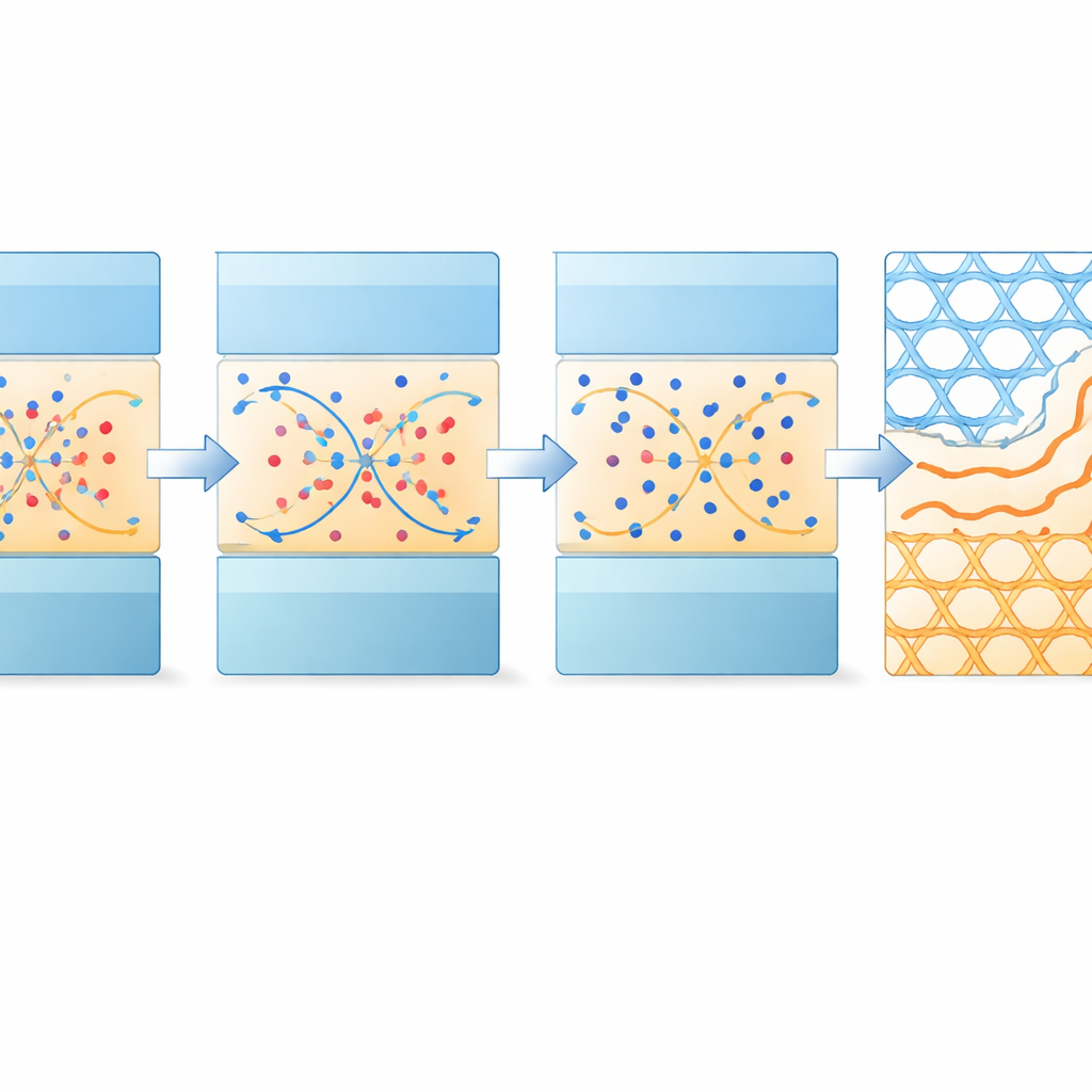
Modern silicon‑on‑insulator wafers are often made by shooting a huge dose of oxygen ions into hot silicon, then baking the wafer at very high temperatures. During this treatment, oxygen atoms rearrange and eventually form a buried silicon dioxide layer—the “insulator”—between the top device layer and the bulk silicon beneath. The exact thickness and sharpness of these layers are crucial: too thin or too rough, and transistors run hot or fail; too thick, and the chip becomes harder to cool and more expensive to make. The problem is that oxygen atoms are constantly moving in and out of the buried region during heating, and until now it has been very difficult to predict precisely where they will end up and how this affects heat transport.
Teaching a model to see atoms like quantum physics
The authors build a computational framework that marries quantum‑accurate physics with deep learning. First, they use demanding quantum‑based simulations to watch individual oxygen ions slam into silicon and come to rest, mimicking the implantation step in the factory. These atomic snapshots then feed a machine‑learning model, called a deep potential, which is trained to reproduce the same forces and energies that full quantum calculations would produce. Once trained, this model can run vastly faster than quantum methods while retaining almost the same accuracy. It can follow oxygen atoms as they wander through silicon and silicon dioxide over much longer times and larger regions than would otherwise be feasible.
Replaying the furnace step and matching real wafers
With this fast yet accurate model in hand, the researchers simulate the high‑temperature “annealing” stage, when implanted wafers are baked to let oxygen redistribute and the buried oxide layer grow. Their calculations produce detailed oxygen‑concentration profiles as a function of depth inside the wafer. By choosing a critical oxygen level that marks the transition from mostly silicon to mostly oxide, they can read off the predicted thicknesses of the surface silicon film and the buried oxide. They then compare these predictions with measurements from real wafers made under many different implantation energies, doses, and thermal cycles. Across eight sample wafers, the simulated and measured layer thicknesses typically differ by less than five percent, showing that the model captures the key atomic movements that define the final device structure.
Zooming in on how heat crosses an invisible border
Beyond structure, the team also tackles how heat moves across the boundary between crystalline silicon and amorphous silicon dioxide—a bottleneck that can limit chip cooling. Using their deep‑learning potential inside a special kind of heat‑flow simulation, they create an idealized, atomically sharp interface and drive heat from one side to the other. By measuring the temperature jump at the boundary and the steady heat flux, they extract the interface thermal resistance, a measure of how strongly the interface blocks heat. Their predicted value lines up more closely with experimental measurements than do earlier simulations based on simpler, empirical models, especially for this tricky mixed crystal‑and‑glass boundary.
What this means for future chip design
Overall, the study turns a complex, multistep manufacturing recipe into a virtual laboratory that links fabrication choices—such as oxygen dose, implantation energy, and annealing temperature—directly to both layer thickness and heat‑flow behavior. For non‑specialists, the key takeaway is that artificial intelligence, when carefully trained on quantum‑level data, can reliably track how individual atoms move and how that motion shapes the performance of full‑scale devices. This approach promises more rational design of silicon‑on‑insulator technologies, helping engineers fine‑tune buried layers and thermal interfaces on a computer screen before committing to costly wafer runs.
Citation: Yan, X., Liu, M., Cheng, W. et al. Deep learning modeling of oxygen redistribution and thermal transport in silicon on insulator and buried oxide layers. Commun Mater 7, 80 (2026). https://doi.org/10.1038/s43246-026-01130-z
Keywords: silicon on insulator, oxygen diffusion, deep learning simulation, thermal interface resistance, molecular dynamics